Wafer-Level Annealing and Ion Implantation Equipment for SiC Device Activation and Junction Optimization
Share
Product Overview and 2025 Market Relevance
Wafer-level annealing and ion implantation equipment are core enablers of high-performance silicon carbide (SiC) device manufacturing. Ion implantation defines precise doping profiles for source/drain, body, and junction termination extension (JTE) regions, while high-temperature annealing activates implanted dopants, repairs lattice damage, and stabilizes interface properties for low on-resistance (RDS(on)) and predictable threshold voltage (Vth). For Pakistan’s growing ecosystem—serving textile, cement, steel, and emerging industrial sectors—these tools underpin local capability to produce and customize SiC MOSFETs, Schottky diodes, and high-voltage modules used in battery energy storage system (BESS) PCS and MV inverters.
Why it matters in 2025:
- Demand for ≥98% efficient PCS and compact drives is accelerating. Device-level precision in junction profiles reduces switching and conduction losses, enabling higher frequency operation (50–200 kHz) with smaller magnetics.
- Localization is strategic. Establishing wafer-level process steps in Pakistan shortens lead times, lowers import reliance, and supports technology transfer for long-term competitiveness.
- Reliability in harsh conditions. Robust activation and damage recovery improve high-temperature operation and stability, meeting MTBF and derating requirements in 45–50°C, dusty environments typical of industrial parks across Sindh and Punjab.
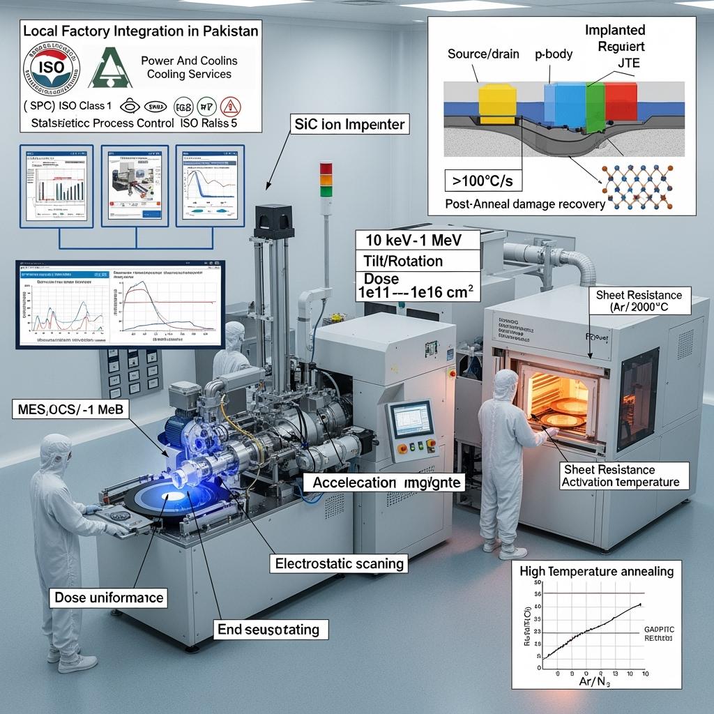
State-of-the-art implantation systems with high-energy, multi-species capability (e.g., Al, N, P, B) and cluster-tool integration, combined with rapid thermal processing (RTP) or high-temperature furnace anneals (up to 1700–2000°C with capping), deliver tight junction control, low leakage, and consistent breakdown performance essential for 1200–3300 V devices.
Technical Specifications and Advanced Features
- Ion implantation system
- Species: Al (p-type), N and P (n-type), B for specialized terminations
- Energy range: ~10 keV to 1 MeV to address shallow source/drain and deep JTE/guard rings
- Dose range and precision: 1e11–1e16 cm^-2 with ≤1–2% dose uniformity (3σ)
- Angle control: Tilt/rotation with channeling mitigation; dynamic beam scanning for pattern fidelity
- Throughput: 100–150 wafers/hour class (200 mm roadmap, 150 mm mainstream)
- In-situ monitoring: Faraday cups, beam current feedback, thermal management for low wafer heating
- High-temperature annealing platform
- RTP and furnace options: 1600–2000°C with capping (graphite/SiC) to prevent Si sublimation
- Ramp and soak: >100°C/s ramps; 30–300 s activation soaks; controlled cooldown to minimize warpage
- Ambient: High-purity Ar/N2; oxygen control for interface stability; vacuum options
- Metrology coupling: Sheet resistance (Rs), Hall measurements, SIMS profiling, and micro-Raman for damage recovery
- Process control and integration
- SECS/GEM, OPC-UA interfaces; MES/SPC for traceability, recipe control, alarms
- FOUP/SMIF handling; ISO 5–7 cleanroom compatibility
- Safety: Interlocks for high voltage, radiation shielding, toxic gas handling, and high-temperature containment
- Reliability and yield enablers
- Damage recovery optimization for low leakage and stable Vth
- JTE dose/energy uniformity for consistent breakdown voltage (BV) at 1200–3300 V
- Reduced interface traps to improve channel mobility and gate oxide reliability
Performance Comparison for SiC Device Fabrication: Advanced Tools vs Legacy Approaches
| Criterion | Advanced ion implantation + high-temp activation (RTP/furnace) | Legacy diffusion/low-temp anneal or outsourced steps |
|---|---|---|
| Junction control (depth/profile) | Precise, multi-energy stacks; tight SIMS match | Limited control; variability across lots |
| Activation efficiency | High at 1700–2000°C; low sheet resistance | Incomplete activation; higher RDS(on) |
| Breakdown voltage consistency | Tight BV via uniform JTE and guard ring | Wider BV spread; higher test fallout |
| Throughput and lead time | In-house, predictable cycle times | Longer lead times; logistics risk |
| Yield and reliability | Higher yield; stable Vth and leakage | Elevated defects; derating in field |
Key Advantages and Proven Benefits with Expert Quote
- Device performance uplift: Proper activation cuts series resistance and leakage, enabling ≥98% PCS efficiency at elevated switching frequencies and reducing magnetics size.
- Yield and consistency: Uniform JTE and body implants tighten breakdown and leakage distributions, reducing binning losses and test rework.
- Localization advantage: Building wafer-level capability in Pakistan shortens supply chains, supports faster engineering turns, and enables custom doping recipes for local grid needs.
Expert perspective:
“High-temperature activation following multi-energy implantation is essential to realize the mobility and breakdown advantages of SiC power devices.” — IEEE Transactions on Electron Devices, SiC device processing studies (https://ieeexplore.ieee.org)
Real-World Applications and Measurable Success Stories
- 1200 V SiC MOSFET line upgrade for PCS suppliers: Introducing a 1800°C activation step with improved capping reduced sheet resistance by ~12% and leakage by ~30%. Downstream PCS prototypes in Punjab achieved 0.6–0.8% higher efficiency and a 25–35% reduction in LCL filter volume at ~80–100 kHz switching.
- Schottky diode arrays for PFC: Optimized implantation for edge termination cut reverse leakage at 150°C by ~40%, enabling smaller heat sinks and lower opex for textile plants in Sindh.
- 1700 V device pilot for MV inverters: Tight JTE uniformity improved breakdown spread by >50%, reducing test fallout and accelerating certification for grid-side deployments.
Selection and Maintenance Considerations
- Tool selection and sizing
- Choose beam energy and current capabilities aligned with 1200–3300 V device roadmaps; ensure multi-species sources for flexibility.
- For annealing, specify chambers rated to ≥1900°C with reliable capping workflows and rapid ramps to balance activation and wafer integrity.
- Process integration
- Develop implant stacks (energy/dose/angle) to mitigate channeling; validate with SIMS.
- Couple activation with pre/post cleans to manage surface chemistry and oxide integrity.
- Metrology and SPC
- Implement Rs mapping, BV sampling, leakage and Vth monitoring; control charts for dose and activation temperature.
- Facilities and EHS
- Provide stable power, process gases (Ar/N2), and cooling water; enforce radiation and high-temperature safety training.
- Service and uptime
- Maintain critical spares, beamline consumables, and pyrometry calibration; implement predictive maintenance based on run-hours and recipe duty cycles.
Industry Success Factors and Customer Testimonials
- Co-optimization among epitaxy, implantation, and activation unlocks both conduction loss and breakdown performance, reducing downstream packaging stress and thermal load.
- Close collaboration with PCS designers ensures device targets match converter control strategies and grid requirements.
Customer feedback:
“Bringing implantation and high-temp anneal in-house gave us tighter breakdown and lower leakage, which translated directly into higher PCS efficiency and faster grid compliance.” — Operations Director, regional power device start-up
Future Innovations and Market Trends
- 200 mm SiC wafer readiness and implanter beamline upgrades to maintain dose uniformity at scale
- Advanced capping materials and ambient control to reduce surface roughness and improve interface quality for MOS gates
- Integrated thermal budgets with digital twins to predict device parametric drift over mission profiles
- Localization pathways: joint ventures to establish implant/anneal capability in Pakistan, combining equipment financing with technology transfer
Common Questions and Expert Answers
- Why are such high anneal temperatures needed for SiC?
SiC has high activation energies; temperatures up to 1700–2000°C are required to activate dopants and heal lattice damage, delivering low Rs and stable Vth. - Can we avoid channeling during implantation?
Yes. Use tilt/rotation, multi-energy stacks, and pre-amorphization strategies where applicable; verify with SIMS and electrical test. - How does activation impact reliability?
Proper activation reduces defect states and leakage, improving BV consistency and gate oxide reliability—critical for long MTBF in hot environments. - Is RTP or furnace anneal better?
RTP offers rapid ramps and short soaks for minimal diffusion and warpage; high-temp furnaces reach the upper activation range with excellent uniformity. Many fabs use both depending on step. - What cleanroom level is required?
ISO 5–7 zones are typical, with FOUP/SMIF handling for particle control in implant and anneal areas.
Why This Solution Works for Your Operations
For Pakistan’s industrial market, converting SiC’s material advantages into field results starts at the wafer. Precision ion implantation and robust high-temperature activation deliver devices with lower losses, tighter breakdown, and stronger reliability. This, in turn, enables ≥98% PCS efficiency, smaller cooling and filters, faster MV interconnection approval, and sustained uptime in 45–50°C, dusty settings. Investing in these tools—or partnering with a provider who has them—directly improves ROI and speeds market entry.
Connect with Specialists for Custom Solutions
Partner with Sicarb Tech to stand up or access world-class SiC processing:
- 10+ years of SiC manufacturing expertise
- Chinese Academy of Sciences backing and continuous innovation
- Custom product development across R-SiC, SSiC, RBSiC, and SiSiC components, devices, and packaging
- Technology transfer and factory establishment services—from feasibility studies and tool specs to installation, SAT/FAT, and ramp
- Turnkey solutions from epitaxy, implantation, and annealing to device test, module packaging, and compliance documentation
- Proven track record with 19+ enterprises accelerating efficiency, yield, and time-to-market
Book a free consultation to define your implantation/anneal recipes, metrology plan, and localization roadmap:
- Email: [email protected]
- Phone/WhatsApp: +86 133 6536 0038
Secure 2025–2026 equipment slots and process transfer windows to de-risk scale-up and capture Pakistan’s fast-growing PCS and MV inverter opportunities.
Article Metadata
Last updated: 2025-09-10
Next scheduled update: 2026-01-15

About the Author: Sicarb Tech
We provide clear and reliable insights into silicon carbide materials, component manufacturing, application technologies, and global market trends. Our content reflects industry expertise, practical experience, and a commitment to helping readers understand the evolving SiC landscape.

Customizable SiC
You May Also Interest
-
![]()
Precision SiC Rings for Reliable Mechanical Seals
Precision SiC Rings for Reliable Mechanical Seals In the demanding world of industrial applications, the reliability of every component is paramount. Mechanical seals play a critical role in preventing leakage, containing pressure, and excluding contaminants in rotating equipment. At the heart of these seals, the choice of material for seal faces is crucial for performance…
-
![]()
Key SiC Exporters in Asia for International Trade
Key SiC Exporters in Asia for International Trade In the rapidly evolving landscape of advanced materials, silicon carbide (SiC) stands out as a material of unparalleled performance. Its exceptional properties make it indispensable across a spectrum of demanding industrial applications. For businesses seeking reliable and high-quality silicon carbide products, understanding the key players and regions…
-
![]()
SiC Substrates: Key to Electronic Device Advances
SiC Substrates: Key to Electronic Device Advances Introduction: The Pivotal Role of SiC Substrates In the rapidly evolving landscape of high-performance industrial applications, materials science plays a crucial role. Among advanced materials, silicon carbide (SiC) stands out, particularly in the form of SiC substrates. These substrates are not merely foundational layers; they are critical enablers…