Wafer-Level Annealing and Ion Implantation Equipment for SiC Junction Activation and Doping Precision
Share
Product Overview and 2025 Market Relevance
Wafer-level annealing and ion implantation equipment are core enablers of high-performance silicon carbide (SiC) power devices, ensuring precise dopant placement and complete junction activation after implantation damage repair. For Pakistan’s industrial market—textile, cement, steel, and emerging sectors—reliable SiC devices underpin efficient 11–33 kV grid-tied photovoltaic inverters and high-duty industrial drives. Achieving ≥98.5% system efficiency, up to 2× power density, and MTBF targets of 200,000 hours starts at the wafer line, where implantation energy, dose uniformity, tilt/rotation control, and post-implant high-temperature anneals determine on-resistance, threshold voltage stability, breakdown integrity, and long-term reliability.
In 2025, Pakistan’s policy direction favors local manufacturing capability and technology introduction. Establishing or partnering for front-end SiC processing capacity—implant and activation anneal—can shorten supply chains, reduce costs, and tailor device characteristics for local ambient heat (45°C+) and dust-prone sites. Modern ion implanters with high-energy options (hundreds of keV to multi-MeV for deep junctions) combined with rapid thermal processing (RTP) or high-temperature furnace anneals (e.g., 1500–1700°C with protective capping) deliver the doping precision and activation ratios necessary for robust 1200V–3300V devices used in medium-voltage topologies.
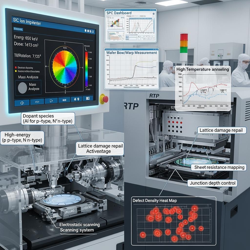
Technical Specifications and Advanced Features
- Ion implantation capabilities:
- Energy range: ~20 keV to >1 MeV (multi-energy stacks for box profiles and graded junctions)
- Dose control: 1e11–1e16 cm⁻² with dose uniformity ≤±1–2% across 150–200 mm wafers
- Species: Al, N, P, B (as appropriate), with charge-state and beam current optimization for throughput
- Angle control: Tilt/rotation for channeling suppression and vertical profile consistency
- Thermal management: Wafer temperature control to mitigate implant-induced defects and manage dopant diffusion
- Wafer-level annealing:
- Temperature capability: Up to ~1700°C with precise ramp/dwell/cool profiles
- Environment: Inert gas, high-purity graphite fixtures, protective capping layers to prevent SiC surface degradation
- Metrology integration: In-line emissivity-corrected pyrometry, IR thermography, and post-anneal sheet resistance mapping
- Uniformity and yield:
- Advanced beamline stabilization and real-time dose monitoring (Faraday cup array, beam profile feedback)
- Statistical process control (SPC) with run-to-run recipe adjustment
- Wafer bow/warp compensation to preserve lithography alignment fidelity
- Data and traceability:
- Full MES connectivity, lot genealogy, parameter logging, and recipe version control
- Defect correlation workflows linking implant/anneal conditions to device parametrics (RDS(on), Vth, BV)
Descriptive Comparison: SiC-Optimized Implant/Anneal vs Conventional Approaches
| Criterion | SiC-optimized implantation and high-temperature activation | Conventional implant with lower-temperature anneal |
|---|---|---|
| Activation efficiency | High activation of dopants with lattice repair | Partial activation; higher series resistance |
| Junction control | Precise depth and profile via multi-energy stacks | Broader profiles, less control at depth |
| Device performance | Lower RDS(on), stable Vth, strong breakdown | Elevated on-resistance, variability |
| Reliability | Improved stability at -40°C to +175°C | Increased drift and early-life variation |
| Yield and uniformity | Tight dose/angle control, ≤±1–2% uniformity | Wider spread, more binning loss |
Key Advantages and Proven Benefits with Expert Quote
- Precise doping profiles: Multi-energy implantation and angular control produce well-defined junctions for 1200V–3300V devices.
- High activation ratios: 1500–1700°C anneals repair lattice damage and activate dopants, minimizing on-resistance and improving conduction efficiency.
- Reliability at temperature: Wafer-level control reduces parameter drift under 45°C+ ambient conditions prevalent in Pakistan’s industrial facilities.
- Throughput with quality: Closed-loop dose and temperature control yield consistent wafers, reducing downstream screening and scrap.
Expert perspective:
“High-temperature activation is essential for SiC to realize its low-loss potential; careful control of implantation profiles and anneal conditions directly translates into converter efficiency and reliability.” — IEEE Power Electronics and Materials Processing literature consensus (ieee.org)
Real-World Applications and Measurable Success Stories
- Medium-voltage PV inverter die: Enhanced activation anneal reduced specific on-resistance (RSP) by ~10–15%, contributing to inverter efficiency ≥98.5% and enabling a 30–40% reduction in cooling volume when paired with optimized packaging.
- Industrial drive switches for steel mills: Tight Vth distribution from improved implant uniformity cut gate-drive margining complexity and reduced field returns under frequent load transients.
- Textile sector VFD modules: Stable breakdown voltage and reduced leakage at high temperature improved uptime during summer peaks and minimized derating events.
Selection and Maintenance Considerations
- Equipment selection:
- Choose implanters with high-energy capability for deep junctions required in high-voltage devices.
- Ensure anneal systems support rapid ramps to ≥1600°C with reliable temperature sensing and surface protection.
- Recipe development:
- Calibrate multi-energy stacks and tilt/rotation to suppress channeling on 4H-SiC crystal orientations.
- Validate carbon-cap or protective coatings to prevent surface step bunching and roughness.
- Metrology plan:
- Implement sheet resistance mapping, SIMS (as available) for profile verification, and post-anneal leakage/breakdown sampling.
- Track wafer bow and defectivity against lithography overlay budgets.
- Environmental robustness:
- Maintain ultra-clean inert atmospheres; monitor oxygen ppm to prevent oxidation.
- Schedule preventive maintenance for beamline optics, pyrometry calibration, and graphite fixture conditioning.
Industry Success Factors and Customer Testimonials
- Co-optimization: Close collaboration between process, device, and packaging teams aligns implant/anneal targets with gate-driver and thermal design requirements, reducing time-to-yield.
- Local capability building: Establishing wafer-level process steps in-region shortens lead times for Pakistan’s MV inverter and drive programs.
Customer feedback:
“After tuning implant angles and adopting higher-temperature activation, our Vth spread tightened and on-resistance fell, improving efficiency and simplifying module binning.” — Process engineering lead, power device manufacturer serving MV inverter market
Future Innovations and Market Trends
- Advanced beamline control with real-time dose mapping and AI-based drift correction
- RTP systems with improved emissivity handling for SiC and adaptive ramp profiles to minimize thermal stress
- Larger wafer formats and automated handling to improve throughput and cost per amp
- Regional partnerships to expand local SiC front-end capability in support of the projected >5 GW MV PV pipeline and a USD 500 million inverter market
Common Questions and Expert Answers
- Why is high-temperature annealing critical for SiC junction activation?
Implantation damages the lattice; annealing at ~1500–1700°C repairs defects and activates dopants, reducing resistance and stabilizing device parameters. - Which dopants are commonly implanted in SiC power devices?
Aluminum for p-type regions; nitrogen (and sometimes phosphorus) for n-type, with energies/doses tailored to target depths and concentrations. - How do implantation tilt and rotation improve results?
They suppress channeling effects in SiC’s crystal lattice, ensuring consistent depth profiles and uniform electrical characteristics across the wafer. - What metrology is recommended post-anneal?
Sheet resistance mapping, leakage and breakdown sampling, and where available, SIMS for dopant profiling; acoustic or optical checks for wafer integrity. - Can these tools support ramp-up to local manufacturing in Pakistan?
Yes. With recipe libraries, SPC, and training, manufacturers can localize critical steps, reducing import dependency while meeting high-voltage device specs.
Why This Solution Works for Your Operations
Precise ion implantation and high-temperature activation annealing are the foundation of low-loss, high-reliability SiC devices. For Pakistan’s 11–33 kV PV and industrial drives, front-end process control translates into measurable field benefits: higher efficiency (≥98.5%), greater power density (up to 2×), smaller cooling systems (about 40% reduction), and longer life in hot, dusty environments. Investing in these capabilities—or partnering with providers who have them—delivers consistent device performance and robust supply for mission-critical applications.
Connect with Specialists for Custom Solutions
Engage with specialists to define the right implantation energies, doses, and anneal profiles for your target devices and applications:
- 10+ years of SiC manufacturing expertise and application engineering
- Backing from a leading research ecosystem for rapid process innovation
- Custom development options across R-SiC, SSiC, RBSiC, and SiSiC material systems
- Technology transfer and factory establishment services, from feasibility to qualification and ramp
- Turnkey solutions spanning materials, device processing, packaging, testing, and integration
- Proven track record with 19+ enterprises delivering performance and ROI
Request a free consultation and a tailored wafer-level process roadmap:
- Email: [email protected]
- Phone/WhatsApp: +86 133 6536 0038
Article Metadata
Last updated: 2025-09-10
Next scheduled update: 2026-01-15

About the Author: Sicarb Tech
We provide clear and reliable insights into silicon carbide materials, component manufacturing, application technologies, and global market trends. Our content reflects industry expertise, practical experience, and a commitment to helping readers understand the evolving SiC landscape.

Customizable SiC
You May Also Interest
-
![]()
Silicon Carbide for Filtration: Revolutionizing Separation in Demanding Environments
In the ever-evolving landscape of industrial processing, the demand for highly efficient, durable, and reliable filtration solutions has never been greater. As industries push the boundaries of temperature, pressure, and chemical aggression, conventional filter materials often fall short. This is where custom silicon carbide (SiC) filtration products emerge as a game-changing technology. Renowned for their…
-
![]()
SiC Academic Research Insights for Industry Use
SiC Academic Research Insights for Industry Use In the relentless pursuit of performance and efficiency across demanding industrial sectors, silicon carbide (SiC) has emerged as a cornerstone material. Its exceptional properties—ranging from unparalleled hardness and wear resistance to superior thermal conductivity and chemical inertness—make it indispensable for high-stakes applications. This blog post delves into the…
-
![]()
Precision SiC Rings for Reliable Mechanical Seals
Precision SiC Rings for Reliable Mechanical Seals In the demanding world of industrial applications, the reliability of every component is paramount. Mechanical seals play a critical role in preventing leakage, containing pressure, and excluding contaminants in rotating equipment. At the heart of these seals, the choice of material for seal faces is crucial for performance…