Arka Yüz Metalizasyonuna Hazırlık ve Düşük Yonga Kesme için Entegre Silisyum Karbür Yonga Levha Kesme ve İnceltme Makineleri
Paylaş
Ürüne Genel Bakış ve 2025 Pazar İlgisi
Silisyum karbür (SiC) için özel olarak üretilmiş entegre gofret kesme ve inceltme makineleri, hassas arka uç hattı (BEOL) hazırlığına olanak tanır; taşlama, gerilim giderme, parlatma ve düşük çip dilimleme; böylece gofretler arka taraf metalizasyonuna, inceltmeye bağlı cihaz performansına ve yüksek verimli kalıp tekilleştirmeye hazır hale gelir. Pil enerji depolama sistemi (BESS) PCS, MV invertörler ve endüstriyel sürücüler sağlayan Pakistan'ın hızlanan güç elektroniği ekosistemi için bu araçlar, pazara sunma süresini kısaltır, cihaz verimini artırır ve yerelleştirme hedeflerini destekler.
SiC'nin sertliği ve kırılganlığı (Mohs ~9,5), mekanik işlemeyi zorlaştırır. Uygunsuz inceltme ve dilimleme, arıza gerilimini düşüren, sızıntıyı artıran ve modül güvenilirliğini düşüren mikro çatlaklara ve yontulmalara neden olur; özellikle Pakistan'ın tekstil, çimento ve çelik tesislerinde yaygın olan 45–50°C ortam sıcaklığı, toz ve titreşim altında. Adaptif taşlama/parlatma, gerilim giderme kimyasalları, gizli/lazer kazıma ve bıçak veya hibrit dilimleme içeren entegre bir hat, kenar bütünlüğünü yüksek ve parçacık kirliliğini düşük tutarak Ag-sinter bağlantısı ve yüksek termal iletkenliğe sahip seramik alt tabakalar (Si3N4/AlN) için uygun kalıplar sağlar.
2025'te, Pakistan yeni enerji depolamada 3–5 GWh ve daha derin endüstriyel elektrifikasyonu hedeflediğinden, SiC gofret hazırlama ve tekilleştirmeye yerel erişim, tedarik direncini artırır, ithalat teslim sürelerini azaltır ve teknoloji transferi girişimleriyle uyum sağlar; doğrudan PCS verimliliğini, güç yoğunluğunu ve MTBF'yi etkiler.
Teknik Özellikler ve Gelişmiş Özellikler
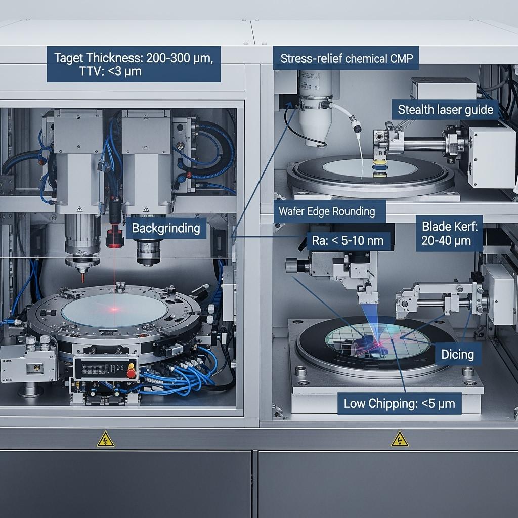
- İnceltme ve düzlük
- Taşlama kalınlık aralığı: 150/200 mm gofretler için tipik olarak 150–350 µm'ye kadar; ultra ince hedefler için gelişmiş taşıyıcılar
- Toplam kalınlık değişimi (TTV): ≤±3–5 µm (parlatma sonrası); sıcaklık kontrollü aynalar aracılığıyla gofret bükülme/eğilme kontrolü
- Yüzey pürüzlülüğü: CMP/parlatma sonrası Ra ≤ 5–10 nm, arka taraf metal yapışmasını ve termal teması optimize etmek için
- Kenar bütünlüğü ve hasar kontrolü
- Gerilim giderme işlemleri: alt yüzey hasarını (SSD) gidermek için ince taşlama + özel bulamaçlarla CMP
- Dilimleme ve modül montajı sırasında çatlak oluşumunu baskılamak için kenar yuvarlama ve pah parlatma
- Dilimleme esnekliği
- Yüzey hasarını azaltmak için gizli lazer kazıma (kızılötesi), ardından bıçak veya yalnızca gizli ayırma
- Ultra ince bıçaklarla (20–40 µm kerf), optimize edilmiş besleme hızları ve soğutucu dağıtımı ile bıçakla dilimleme
- Tipik yontulma: üst/alt kenarlarda ≤3–5 µm; aktif yıkama/kurutma ile düşük parçacık üretimi
- Metroloji ve SPC
- Hat içi kalınlık, TTV ve eğilme haritalaması; optik kenar denetimi; otomatik görüntü analizi ile yontulma ölçümü
- Arka taraf metal yapışma gereksinimleriyle uyumlu parçacık sayaçları ve dilimleme sonrası temizlik kontrolleri
- Otomasyon ve kirlilik kontrolü
- FOUP/SMIF kullanımı; ISO 5–7 temiz bölgeler; HEPA aşağı akışı; DI su geri kazanımı ve filtrasyonu
- SECS/GEM, OPC-UA bağlantısı; reçete/sürüm kontrolü ve parti soy ağacı
- Güvenlik ve ÇYS
- Lazer sınıfı güvenlik kilitlemeleri; soğutucu/kimyasal izleme; acil durum durdurmaları; ergonomik bakım erişimi
Karşılaştırmalı Genel Bakış: Entegre SiC İnceltme/Dilimleme ve Geleneksel Silikon Hatları
| Kriter | Entegre SiC gofret kesme ve inceltme makineleri | Geleneksel silikon odaklı araçlar |
|---|---|---|
| SiC'de kenar yontulması | Gizli + optimize bıçak ile ≤3–5 µm | Tipik olarak >10 µm; daha yüksek çatlak riski |
| Yüzey altı hasar giderme | Özel SiC gerilim giderme ve CMP | Sınırlı; daha yüksek SSD kalır |
| TTV ve eğilme kontrolü | Sıcaklık kontrollü aynalarla sıkı kontrol | Sert, kırılgan SiC için daha az etkili |
| Arka yüzey metalizasyon hazırlığı | Ra ≤ 5–10 nm; temiz yüzey kimyası | Genellikle ek yeniden işleme gerekir |
| Verim ve güvenilirlik etkisi | Daha yüksek kalıp verimi; daha iyi BV ve sızıntı | Artan düşüş ve saha riski |
Uzman Teklifi ile Temel Avantajlar ve Kanıtlanmış Faydalar
- Daha yüksek cihaz verimi ve güvenilirliği: Düşük SSD inceltme ve düşük çip dilimleme, sürüklenme bölgelerini ve sonlandırma bütünlüğünü koruyarak arıza gerilimi (BV) dağılımlarını sıkılaştırır ve sızıntıyı düşürür.
- Arka taraf metal işlem hazırlığı: Kontrollü pürüzlülük ve temiz yüzeyler, metal yapışmasını ve termal yol tutarlılığını iyileştirerek Ag-sinter bağlantısını ve yüksek MTBF'yi destekler.
- Yerelleştirme ve hız: Ülke içindeki gofret hazırlığı, lojistik riskini azaltır, hızlı mühendislik dönüşlerini destekler ve Pakistan'ın endüstriyel yükseltme hedefleriyle uyum sağlar.
Uzman bakış açısı:
“SiC’s mechanical hardness and brittleness demand specialized thinning and dicing strategies; controlling sub-surface damage and edge chipping is critical for high-voltage device yield and reliability.” — IEEE Transactions on Electron Devices, SiC back-end processing insights (https://ieeexplore.ieee.org)
Gerçek Dünya Uygulamaları ve Ölçülebilir Başarı Hikayeleri
- 1200 V cihazlar için 150 mm MOSFET hattı: Optimize CMP ile gizli kazıma + bıçak dilimlemeye geçiş, ortalama kenar yontulmasını ~9 µm'den ~3 µm'ye düşürdü ve sızıntı ile ilgili test düşüşünü ~ azalttı. Pencap'taki dağıtımlarda aşağı yönlü PCS verimliliği, daha sıkı cihaz dağılımları nedeniyle ~%0,4–0,6 iyileşti.
- Endüstriyel sürücüler için 1700 V JBS diyotları: TTV ±3 µm'ye sıkılaştırıldı ve arka taraf Ra ~7 nm, arka taraf metal yapışmasını iyileştirdi; Sind tekstil fabrikalarında sızıntı ile ilgili arızalar için saha iade oranı > düştü.
- 200 mm pilot hazırlığı: 200 mm taşıyıcılar ve ayna soğutması için entegre hat yenilendi, eğilme/eğilmeyi stabilize etti, MV invertör cihazları için tutarlı BV tekdüzeliği ve ~ azaltılmış kutu yayılması ile ilk gofret demolarına olanak sağladı.
Seçim ve Bakımla İlgili Hususlar
- İşlem reçetesi tasarımı
- SSD'yi en aza indirmek için CMP'den sonra çok aşamalı taşlama (kaba → ince) seçin; uygun olduğunda kesit ve mikro-Raman/PL ile doğrulayın.
- Bıçak tipini, besleme hızını ve soğutucu kimyasını ayarlayın; gizli kullanılıyorsa, kazıma derinliğini cadde genişliğine ve gofret kalınlığına göre optimize edin.
- Metroloji ve SPC
- TTV'yi, Ra'yı, yontulma histogramlarını ve parçacık sayımlarını partiden partiye izleyin; otomatik alarmlarla kontrol limitleri uygulayın.
- Kenarları yüksek çözünürlüklü optiklerle inceleyin; geri bildirim için yontulmayı cihaz sızıntısı/BV yayılmasıyla ilişkilendirin.
- Sarf malzemesi yönetimi
- Bıçak ömrü kayıtlarını, bulamaç filtrasyonunu ve DI su kalitesini koruyun; lazerler, optikler ve aynalar için yedek parça planlayın.
- Temizlik ve güvenlik
- Dilimleme sonrası sağlam temizleme/kurutma sağlayın; arka taraf metalizasyonunu veya sinterlemeyi bozabilecek kalıntıları izleyin.
- Lazer güvenliği ve kimyasal kullanım SOP'larına uyun; operatör eğitimi sağlayın.
- Yukarı/aşağı akış ile entegrasyon
- Epitaksi düz yönelimi, implantasyon/tavlama planları ve arka taraf metal yığınlarıyla hizalayın; taşıyıcı uyumluluğunu ve eğrilik özelliklerini sağlayın.
Sektör Başarı Faktörleri ve Müşteri Görüşleri
- Cihaz, işlem ve paketleme ekipleri arasındaki yakın işbirliği esastır; kenar bütünlüğü ve TTV, Ag-sinter bağlantı verimini ve modül termal direncini doğrudan etkiler.
- Veri odaklı geri besleme döngüleri (elektriksel test KPI'lerine SPC), yeniden işleme sayısını azaltır ve programları stabilize eder.
Müşteri geri bildirimi:
“Entegre SiC inceltme ve gizli dilimleme hattı, sızıntı düşüşümüzü yarıya indirdi ve arka taraf metal yapışmasını tutarlı hale getirdi. PCS modüllerimiz, ilk çalıştırmada termal ve şebeke testlerinden geçti.” — Operasyon Müdürü, Pakistan merkezli cihaz fabrikası ortağı
Gelecekteki Yenilikler ve Pazar Eğilimleri
- Gelişmiş taşlama tekerlekleri, iyileştirilmiş ayna soğutması ve yapay zeka destekli reçete ayarlaması ile 200 mm SiC hazırlığı
- Mikro çatlakları daha da bastırmak için hibrit lazer teknolojileri (ultra hızlı femtosaniye)
- 0
- Pakistan'da Yerelleştirme: yonga hazırlama hücreleri kurmak için ekipman finansmanı, işgücü eğitimi ve MES entegrasyonu ile ortak girişimler
Sık Sorulan Sorular ve Uzman Yanıtları
- SiC için neden gizli kazıma + bıçak tercih ediliyor?
Gizli kazıma, bıçakla ayırma sırasında daha düşük mekanik gerilime izin vererek yongayı kesme hatları boyunca önceden zayıflatır; bu da yongalanmayı ≤3–5 µm'ye düşürür. - Arka yüzey metallendirmesi için hangi TTV kabul edilebilir?
Çoğu 1200–1700 V cihaz için, düzgün metal kalınlığı, ambalajlamada iyi düzlemsellik ve tahmin edilebilir termal yollar sağlamak için TTV ≤±3–5 µm hedeflenir. - İnceltme güvenilirliği nasıl etkiler?
Düşük SSD inceltme, termal döngü altında yayılabilecek, BV kararlılığını ve sızıntıyı, özellikle yüksek ortam sıcaklıklarında iyileştiren mikro çatlakları azaltır. - Mevcut silikon kesme araçları SiC'yi işleyebilir mi?
Güvenilir bir şekilde değil. SiC, düşük yonga sonuçları elde etmek için özel bıçaklar, soğutucu teslimatı, pens sıcaklık kontrolü ve genellikle gizli/lazer yardımı gerektirir. - Arka yüzey metali öncesinde ne gibi bir temizliğe ihtiyaç vardır?
Düşük partikül sayıları, minimum kalıntılar ve 5–10 nm aralığında Ra tipiktir; kesim sonrası temizleme ve yüzey aktivasyon adımları önerilir.
Bu Çözüm Operasyonlarınız İçin Neden İşe Yarıyor?
Pakistan'ın SiC cihaz yol haritası için, sağlam yonga inceltme ve düşük yonga kesimi vazgeçilmezdir. Entegre makineler, arka yüzey metallendirme hazırlığı, sıkı TTV ve bozulmamış kenarlar sunar; sızıntıyı ve BV yayılımını azaltır, yonga verimini artırır ve güvenilir Ag-sinter modül montajını sağlar. Bunun karşılığı daha hızlı sertifikasyon, daha yüksek PCS verimliliği (≥), kompakt ambalajlama ve 45–50°C, tozlu endüstriyel ortamlarda uzun saha ömrüdür.
Özel Çözümler için Uzmanlarla Bağlantı Kurun
SiC arka ucunuzu Sicarb Tech ile ölçeklendirin:
- 10+ yıllık SiC üretim uzmanlığı
- Süreç ve metroloji inovasyonu için Çin Bilimler Akademisi desteği
- R-SiC, SSiC, RBSiC, SiSiC malzemeleri ve komple epi-modül akışları genelinde özel geliştirme
- Pakistan için ekipman özellikleri, SOP'lar, eğitim, SAT/FAT ve MES entegrasyonu dahil olmak üzere teknoloji transferi ve fabrika kurulum hizmetleri
- Epitaksi ve implantasyondan yonga hazırlama, arka yüzey metali, cihaz testi ve modül ambalajlamaya kadar anahtar teslim çözümler
- Daha yüksek verim, daha sıkı BV ve daha hızlı pazara sunma sağlayan 19'dan fazla kuruluşla kanıtlanmış bir geçmiş
İnceltme/kesme tarifleri, metroloji planları ve yerelleştirme yol haritaları için ücretsiz bir danışma talep edin:
- E-posta: [email protected]
- Telefon/WhatsApp: +86 133 6536 0038
Ölçeklendirme riskini azaltmak ve Pakistan'ın büyüyen PCS ve MV invertör fırsatlarını yakalamak için 2025–2026 ekipman yuvalarını ve süreç transfer pencerelerini güvence altına alın.
Makale Meta Verileri
Son güncelleme: 2025-09-10
Bir sonraki planlı güncelleme: 2026-01-15

About the Author: Sicarb Tech
We provide clear and reliable insights into silicon carbide materials, component manufacturing, application technologies, and global market trends. Our content reflects industry expertise, practical experience, and a commitment to helping readers understand the evolving SiC landscape.

Customizable SiC
You May Also Interest
-
![]()
SiC Alt Tabakalar: Elektronik Cihaz Gelişmelerinin Anahtarı
SiC Alt Tabakalar: Elektronik Cihaz Gelişmelerinin Anahtarı Giriş: SiC Alt Tabakaların Önemli Rolü Yüksek performanslı endüstriyel uygulamaların hızla gelişen ortamında, malzeme bilimi çok önemli bir rol oynamaktadır. Gelişmiş malzemeler arasında silisyum karbür (SiC), özellikle SiC alt tabakalar şeklinde öne çıkmaktadır. Bu alt tabakalar sadece temel katmanlar değildir; bunlar kritik sağlayıcılardır...
-
![]()
Üniversite Araştırma Bağlantıları Aracılığıyla SiC İnovasyonu
Üniversite Araştırma Bağlantıları Aracılığıyla SiC İnovasyonu Gelişmiş malzemelerin hızla gelişen manzarasında, özel silisyum karbür (SiC) gerçek bir oyun değiştirici olarak öne çıkıyor. Eşsiz özellikleri, onu yarı iletken üretiminin en gelişmiş teknolojisinden havacılık ve nükleer enerjinin aşırı ortamlarına kadar, çok çeşitli zorlu endüstriyel uygulamalarda vazgeçilmez hale getiriyor. Ancak ne...
-
![]()
Güç Elektroniği Mükemmelliği için Yeni Nesil SiC Gofretler
Güç Elektroniği Mükemmelliği için Yeni Nesil SiC Gofretler Giriş: Modern Güç Elektroniğinde SiC Gofretlerin Önemli Rolü Güç elektroniği sistemlerinde daha yüksek verimlilik, artırılmış güç yoğunluğu ve üstün performans arayışı, silisyum karbürün (SiC) dönüştürücü bir malzeme olarak öne çıkmasına neden olmuştur. SiC tabanlı güç cihazları için temel alt tabakalar olan SiC gofretler, ...