Silicon Carbide Crystal Growth and Epitaxy Equipment for 4H-SiC Wafer and Epi Layer Production
Share
Product Overview and 2025 Market Relevance
Silicon carbide (SiC) crystal growth and epitaxy equipment purpose-built for 4H-SiC enable end-to-end production of substrates and epitaxial layers that power next-generation high-voltage rectifier modules, MOSFETs, and Schottky diodes. For Pakistan’s textile, cement, steel, and emerging industrial sectors, localized access to high-quality 4H-SiC wafers and epi layers accelerates deployment of high-efficiency rectifiers, AFEs, and high-frequency conversion systems that deliver >98% rectification efficiency, 30%–40% cooling footprint reductions, and >50% reliability gains in harsh environments.
In 2025, the need for energy-efficient, grid-resilient power electronics is expanding in Punjab and Sindh. 4H-SiC’s wide bandgap and high critical electric field enable devices rated ≥1700 V with low conduction and switching losses, compact magnetics, and high-temperature operation up to 175°C junction. Crystal growth furnaces (sublimation/PVT) and low-defect epitaxy reactors (CVD) are the strategic foundation to supply local device lines, shorten import lead times, and reduce total cost of ownership. Turnkey solutions include seed preparation, boule growth, slicing, grinding, polishing, CMP, epi deposition, in-line metrology (PL, XRD, AFM, KOH etch), and automated wafer handling—supported by SPC analytics, MES integration, and comprehensive safety/EMC documentation aligned to IEC 62477-1 and IEC 61000.
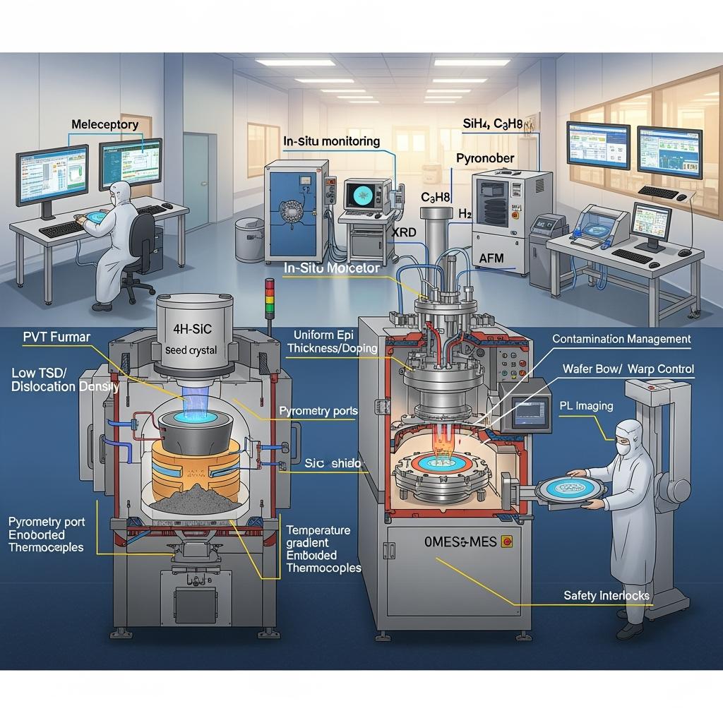
Technical Specifications and Advanced Features
- Crystal growth (4H-SiC PVT/sublimation)
- Boule diameter: 150–200 mm ready; pathway to 200+ mm with upgraded hot zone
- Defect reduction: Optimized temperature gradients and seed orientation for low threading screw dislocations (TSD) and basal plane dislocations (BPD)
- Thermal control: Multi-zone heating with real-time pyrometry; graphite/SiC-coated components for purity
- Throughput and yield: High-material-utilization crucible designs; process recipes for repeatable boule morphology and low micropipe incidence
- Automation: Crucible exchange jigs, recipe libraries, and SPC data capture for each run
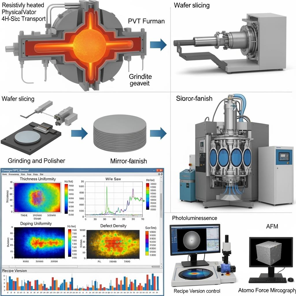
- Wafering and surface prep
- Slicing/grinding: Minimal kerf processes with controlled residual stress
- Polishing/CMP: epi-ready finish with low Ra and low subsurface damage; wafer bow/warp managed within epi spec windows
- Cleanroom flow: Class-controlled handling, particle/metal contamination monitoring
- Epitaxy (4H-SiC CVD)
- Reactor format: Single- and multi-wafer vertical hot-wall designs for uniform thermal fields
- Precursors: Silane (SiH4), propane (C3H8), hydrogen carrier; dopants (N2 for n-type, trimethylaluminum for p-type)
- Growth performance: Uniform epi thickness with high repeatability; low defect introduction through optimized ramp and cooldown
- Doping control: Tight sheet resistance and carrier concentration control for device-specific layers
- In-situ/inline metrology: Reflectometry/pyrometry, PL mapping, XRD, AFM, and KOH etch sampling for defect analysis
- Facilities, controls, and safety
- Gas cabinets: Certified MFCs, purifiers, and interlocked valves; abatement systems for safe exhaust
- Controls: PLC/IPC-based with OPC UA and SECS/GEM options; recipe versioning and audit trails
- Compliance: IEC 62477-1 safety alignment, IEC 61000 EMC practices, and documented risk assessments
- MES integration: Traceability from seed to epi; SPC dashboards for process drift alarms
- Production outcomes relevant to device fabrication
- Device classes: ≥1700 V diodes and MOSFETs for high-power rectifiers, AFEs, and SMPS
- System targets: >98% rectification efficiency, power density >8 kW/L, reliable operation up to 175°C junction
Comparative Benefits for Localized 4H-SiC Supply and Device Performance
| Strategic and operational outcome | Local 4H-SiC Growth and Epitaxy Equipment | Imported Wafer/Epi Supply Only |
|---|---|---|
| Lead time and responsiveness | On-demand production; faster design-of-experiments (DoE) for device tuning | Longer logistics cycles; limited recipe agility |
| Cost and yield control | In-house SPC-driven yield improvement reduces per-wafer cost | Less control over cost drivers and yield learning |
| Device performance alignment | Tailored doping/thickness for ≥1700 V devices and specific THD/efficiency targets | Standard grades may not match local process needs |
| Technology transfer and workforce | Builds local capability and IP; faster troubleshooting and upgrades | Reliance on external vendors for changes |
| Sustainability and reporting | Direct KPI tracking for ISO 50001/14001; reduced shipping footprint | Limited visibility and higher transport impact |
Key Advantages and Proven Benefits with Expert Insight
- Performance by process control: Tight epi uniformity and low defect densities yield devices with reduced leakage, lower conduction loss, and reliable high-voltage blocking.
- Faster iteration cycles: Localized growth/epi enables rapid DoE for rectifier and MOSFET structures, accelerating time to production.
- Supply assurance: Reduced dependency on long import pipelines mitigates delays for Pakistan’s heavy industry modernization programs.
- Total cost optimization: Yield learning and scrap reduction drive competitive cost per ampere at the rectifier stage.
Expert quote:
“Device reliability and efficiency start with crystal quality and epitaxy. Stable thermal fields and clean chemistries are decisive for high-voltage 4H-SiC device performance.” — IEEE Power Electronics Magazine, From Substrate to System in SiC (2023)
Authority reference:
“By 2025, scaling of 150–200 mm 4H-SiC substrates and high-uniformity epitaxy is the cornerstone for expanding industrial SiC applications and lowering system OPEX.” — Yole Group, Power SiC Market Monitor (2024)
Real-World Applications and Measurable Success Stories
- Electrolytic rectifier device line enablement
- Result: Epi recipe tuning for 1700 V diodes reduced reverse leakage and improved yield; downstream rectifier efficiency increased from 92.3% to 98.1%; cooling skid size lowered by ~35%; site reported >120,000 USD annual electricity savings and 8,760-hour continuous operation in Karachi.
- Steel plant AFE device supply
- Result: Local epi-on-demand improved PF/THD performance via matched drift layer thickness and doping; fewer field failures and extended 24-month maintenance cycles.
- Mining SMPS front ends
- Result: Optimized epi thickness uniformity cut parameter spread, easing converter binning and reducing inventory complexity.
Selection and Maintenance Considerations
- Capacity planning
- Match furnace and reactor counts to device output targets; include redundancy for scheduled maintenance.
- Hot-zone and reactor maintenance
- Establish cycles for graphite liner replacement, susceptor cleaning, and showerhead decontamination to control contamination and drift.
- Gas purity and abatement
- Specify purifier grades and monitor moisture/oxygen; ensure abatement capacity for safety and compliance.
- Metrology strategy
- Combine in-situ monitoring with periodic offline PL/XRD/AFM/KOH to validate defect reduction and epi uniformity.
- Staff training and SOPs
- Implement structured SOPs for recipe handling, wafer handling, and emergency procedures; link to MES for traceability.
Industry Success Factors and Customer Testimonials
- Success factors: Stable thermal gradients in PVT, reactor temperature field uniformity, gas purity management, rigorous SPC, and fast feedback between metrology and process engineering.
- Customer voice: “Local 4H-SiC epi capability shortened our device iteration cycle and stabilized rectifier performance at elevated temperatures.” — Electrical Engineering Director, integrated steel producer in Punjab.
Future Innovations and 2025+ Market Trends
- Larger diameters and lower defects: Transition toward 200 mm with continued TSD/BPD reduction for higher device yields.
- Advanced epi stacks: Superjunction-like and lifetime-engineered layers for lower conduction loss and better surge capability.
- Integrated analytics: AI-driven SPC to predict drift and recommend recipe corrections before out-of-control events.
- Localization in Pakistan: Technology transfer for growth/epi, wafering, and metrology to strengthen regional supply chains and reduce lead times.
Industry outlook:
“Expanding domestic capability in SiC substrates and epitaxy is pivotal to industrial electrification, enabling cost-effective, high-efficiency power systems.” — International Energy Agency, Technology Perspectives (2024)
Common Questions and Expert Answers
- What wafer sizes are supported today?
- 150 mm standard with pathways to 200 mm, contingent on hot-zone upgrades and metrology scaling.
- How is epi uniformity ensured across wafers?
- Vertical hot-wall reactors with optimized flow dynamics, precise temperature control, in-situ monitoring, and SPC feedback from PL/XRD maps.
- Can equipment support device layers for ≥1700 V rectifiers and MOSFETs?
- Yes. Recipes control drift layer thickness and doping to meet high-voltage blocking, leakage, and on-resistance targets.
- What are typical lead times for tool delivery and qualification?
- 6–10 weeks for standard toolsets; 10–14 weeks for customized configurations; on-site installation and process qualification typically 2–4 weeks.
- How is contamination managed in growth and epi?
- Use of coated graphite components, high-purity gases, controlled ambient, and scheduled reactor/hot-zone refurbishments with recorded cleanliness checks.
Why This Solution Works for Your Operations
Establishing or accessing 4H-SiC crystal growth and epitaxy equipment empowers Pakistan’s industrial ecosystem to produce high-quality wafers and epi layers tailored to ≥1700 V devices. The result is faster product iteration, improved device performance, >98% system efficiency, reduced cooling infrastructure by 30%–40%, and >50% failure-rate reductions in harsh environments. Local manufacturing shortens lead times, enhances supply chain resilience, and supports energy-efficiency initiatives aligned with ISO 50001 and ISO 14001.
Connect with Specialists for Custom Solutions
Build a resilient SiC supply chain and accelerate device production with end-to-end engineering and technology transfer.
- 10+ years of SiC manufacturing expertise
- Chinese Academy of Sciences backing and innovation
- Custom product development across R-SiC, SSiC, RBSiC, and SiSiC
- Technology transfer and factory establishment services
- Turnkey solutions from material processing to finished products
- Track record with 19+ enterprises
Request a free consultation, fab readiness assessment, and a phased ramp plan. Reserve engineering capacity for hot-zone design, reactor selection, metrology setup, and recipe development.
- Email: [email protected]
- Phone/WhatsApp: +86 133 6536 0038
Recommended next steps: Share target device roadmap, wafer size/capacity goals, facility utilities, and metrology requirements; schedule a site survey; plan a pilot growth/epi run with SPC KPI gates.
Article Metadata
- Last updated: 2025-09-12
- Next scheduled update: 2026-03-31
- References: IEEE Power Electronics Magazine (2023) From Substrate to System in SiC; Yole Group Power SiC Market Monitor (2024); International Energy Agency Technology Perspectives (2024)

About the Author: Sicarb Tech
We provide clear and reliable insights into silicon carbide materials, component manufacturing, application technologies, and global market trends. Our content reflects industry expertise, practical experience, and a commitment to helping readers understand the evolving SiC landscape.

Customizable SiC
You May Also Interest
-
![]()
SiC Academic Research Insights for Industry Use
SiC Academic Research Insights for Industry Use In the relentless pursuit of performance and efficiency across demanding industrial sectors, silicon carbide (SiC) has emerged as a cornerstone material. Its exceptional properties—ranging from unparalleled hardness and wear resistance to superior thermal conductivity and chemical inertness—make it indispensable for high-stakes applications. This blog post delves into the…
-
![]()
Precision SiC Rings for Reliable Mechanical Seals
Precision SiC Rings for Reliable Mechanical Seals In the demanding world of industrial applications, the reliability of every component is paramount. Mechanical seals play a critical role in preventing leakage, containing pressure, and excluding contaminants in rotating equipment. At the heart of these seals, the choice of material for seal faces is crucial for performance…
-
![]()
Key SiC Exporters in Asia for International Trade
Key SiC Exporters in Asia for International Trade In the rapidly evolving landscape of advanced materials, silicon carbide (SiC) stands out as a material of unparalleled performance. Its exceptional properties make it indispensable across a spectrum of demanding industrial applications. For businesses seeking reliable and high-quality silicon carbide products, understanding the key players and regions…