Silicon Carbide Dicing and Wafer Thinning Equipment for Backside Metallization and High-Yield Processing

Share
Product Overview and 2025 Market Relevance
Silicon carbide (SiC) dicing and wafer thinning equipment enables high-yield, high-throughput back-end processing for power devices destined for 11–33 kV grid-tied inverters and industrial drives in Pakistan’s textile, cement, and steel sectors. Purpose-built grinders, CMP/etch tools, stealth laser or blade dicing systems, and stress-relief modules deliver precise wafer thickness control, minimal chipping, and pristine backside surfaces for robust metallization and ohmic contact formation. The result is lower series resistance, improved thermal performance, and enhanced module reliability at operating temperatures up to +175°C, supporting ≥98.5% inverter efficiency and up to 2× power density in hot (45–50°C) and dusty environments across southern Pakistan.
In 2025, growth in medium-voltage photovoltaic deployments (over 5 GW expected in five years) and industrial electrification demands localized, high-yield SiC manufacturing steps. Advanced thinning to 120–250 µm for discrete die and 200–350 µm for large-area chips reduces thermal path length and module stack height. Dicing platforms that manage SiC’s hardness and brittleness—using optimized blade chemistries, stealth laser scribing, or hybrid processes—protect edge integrity, a key determinant of breakdown voltage and long-term leakage stability. Integrating plasma descum, backside implant/anneal compatibility, and controlled roughness for metallization adhesion ensures clean, repeatable back-end processes aligned with high-reliability packaging flows.
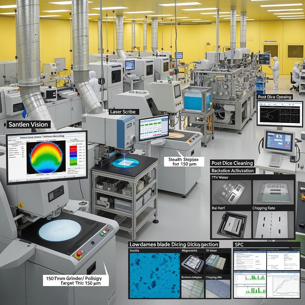
Technical Specifications and Advanced Features
- Wafer thinning and surface engineering
- Target thickness: 120–350 µm (application-dependent); Total Thickness Variation (TTV) ≤ 5–10 µm
- Grinder/CMP: Diamond wheel chemistries optimized for SiC; optional CMP or plasma etch to relieve subsurface damage
- Backside roughness: Tunable Ra ~5–50 nm for metallization adhesion vs. ohmic contact resistance
- Dicing technologies
- Stealth laser scribing + blade break/dice hybrid for minimal edge damage and narrower streets
- High-rigidity spindles and optimized diamond blades for SiC; coolant chemistry controlling debris and thermal shock
- Real-time chipping detection, kerf monitoring, and adaptive feed control to maintain low-defect edges
- Backside metallization readiness
- Surface activation: Oxygen/argon plasma to remove residues and improve adhesion
- Metallization compatibility: Ti/Ni/Ag, Ti/Ni/Au, or Ni/Ag stacks; thermal budgets aligned with prior implant/anneal
- Cleanliness: Megasonic DI, low-ionic contamination, and particle control to Class 1000 or better around deposition
- Metrology and analytics
- In-line thickness mapping, bow/warp measurement, and edge inspection (SEM-ready sample workflow)
- SPC with control charts for TTV, edge chipping percentage, die strength (4-point bend proxy), and metal sheet resistance after deposition
- Throughput and automation
- Cassette-to-cassette handling; recipe-driven layer stacks and street patterns
- MES connectivity for lot traceability, barcode/RFID tracking, and yield dashboards
- Environmental robustness for local deployment
- HEPA-filtered enclosures, dust extraction for grinding/dicing, and corrosion-resistant components for coastal humidity scenarios
- Preventive maintenance schedules and spare kits suitable for regional service logistics
Descriptive Comparison: SiC-Optimized Thinning/Dicing vs Generic Silicon Back-End Lines
| Criterion | SiC-optimized thinning and dicing line | Generic silicon back-end line |
|---|---|---|
| Edge quality and chipping | Stealth/hybrid processes with adaptive control achieve very low chipping | Higher chipping and microcracks on hard/brittle SiC |
| Thickness and TTV | 120–350 µm with TTV ≤ 5–10 µm | Limited control at SiC hardness; larger TTV |
| Backside metallization readiness | Plasma activation, low-damage surfaces, cleanroom-compatible flow | Residual damage and contamination risk |
| Yield on large die | Higher die strength and breakdown integrity | Increased edge defects and leakage drift |
| Uptime in dusty environments | HEPA and dust extraction tuned for abrasive debris | Fouling and accelerated tool wear |
Key Advantages and Proven Benefits with Expert Quote
- Higher device yield: Low-damage thinning and controlled dicing minimize edge defects that trigger leakage and premature breakdown, boosting wafer-to-die yield.
- Improved thermal and electrical performance: Precise thickness control reduces thermal impedance and on-state resistance losses after backside metallization, contributing to ≥98.5% system efficiency.
- Reliability at high ambient: Clean backside interfaces and robust edges enhance long-term stability in 45–50°C environments and under thermal cycling in fielded modules.
- Faster time-to-market: Automated metrology and SPC accelerate root-cause analysis and process tuning for Pakistan’s MV PV and industrial programs.
Expert perspective:
“Edge integrity and backside surface condition are decisive for SiC device reliability. Optimized thinning and dicing processes directly improve breakdown behavior and long-term leakage stability.” — IEEE power device fabrication guidance (ieee.org)
Real-World Applications and Measurable Success Stories
- MV PV MOSFET production: Switching from blade-only to stealth-hybrid dicing reduced edge chipping defects by ~60%, increasing good die per wafer and enabling consistent breakdown across lots used in ≥98.5% efficient inverters.
- Textile and steel drive diodes: Controlled backside roughness and Ti/Ni/Ag stacks lowered contact resistance variability, improving module current sharing and reducing thermal hotspots.
- Large-area module dies: TTV improvement from ~15 µm to ≤7 µm improved attach planarity, reducing voids and enhancing power cycling life in Si3N4/AlN-based packages.
Selection and Maintenance Considerations
- Process definition
- Select target thickness based on thermal simulations and package stack-up; define TTV and bow limits for die attach.
- Choose dicing method: stealth-hybrid for large die and tight kerfs; optimized blade-only for cost-sensitive small die.
- Consumables and parameters
- Match diamond wheel and blade specifications to wafer hardness and thickness; manage coolant chemistry and flow to minimize thermal shock.
- Tune laser power, focus depth, and scan pitch to confine damage below the street.
- Cleanliness and metrology
- Incorporate megasonic cleaning and plasma descum before metallization; validate with surface analysis (e.g., XPS, contact angle).
- Monitor edge defects via automated optical inspection and periodic SEM sampling.
- Tool health in dusty regions
- Enforce HEPA maintenance intervals; track spindle vibration and coolant filtration differentials; maintain spare parts inventory locally.
Industry Success Factors and Customer Testimonials
- Co-optimization with epitaxy and metallization ensures backside dopant activation and contact formation are not compromised by mechanical damage.
- Early DOE on roughness vs. contact resistance and die strength establishes robust process windows.
Customer feedback:
“Stealth scribing plus optimized grinding cut our edge-related failures and stabilized contact resistance. Our MV inverter modules now maintain tighter parameter distributions across production.” — Operations director, regional power device maker
Future Innovations and Market Trends
- Laser stealth advancements enabling narrower streets and higher die per wafer without sacrificing strength
- Hybrid plasma/CMP finishes to further reduce subsurface damage prior to metallization
- Inline machine learning vision for real-time chipping prediction and adaptive feed control
- Localized back-end lines and training programs aligned with Pakistan’s approximately USD 500 million inverter market and >5 GW MV PV buildout
Common Questions and Expert Answers
- What wafer thickness should I target for MV SiC devices?
Typical ranges are 150–250 µm for large MOSFETs/diodes to balance thermal performance and die strength; finalize via thermal-mechanical simulation and attach process limits. - How does stealth dicing improve yield?
It creates internal modified layers that guide crack propagation, reducing surface chipping and microcracks, which improves edge robustness and breakdown consistency. - What backside roughness is optimal for metallization?
Ra in the 10–30 nm range often balances adhesion and low contact resistance; verify with your metal stack and anneal profile. - How can I prevent dust-related tool degradation?
Use HEPA-filtered enclosures, scheduled filter changes, and coolant filtration; monitor spindle vibration and implement predictive maintenance. - Is the process compatible with high-temperature activation anneals?
Yes. Thinning/dicing is sequenced to avoid damage to activated regions; plasma cleans ensure metallization adhesion without degrading prior implants/anneals.
Why This Solution Works for Your Operations
SiC-specific thinning and dicing equipment convert advanced epitaxy and device design into high-yield, reliable die suitable for MV PV and industrial drives in Pakistan. By safeguarding edge integrity, controlling thickness and TTV, and preparing clean backsides for metallization, you realize ≥98.5% efficiency, up to 2× power density, and long service life in hot, dusty environments—reducing total cost and accelerating deployment.
Connect with Specialists for Custom Solutions
Build a high-yield SiC back-end line with an end-to-end partner:
- 10+ years of SiC manufacturing expertise
- Backing from a leading research ecosystem driving innovations in thinning, dicing, and metallization
- Custom product development across R-SiC, SSiC, RBSiC, and SiSiC for thermal and structural integration
- Technology transfer and factory establishment services for local back-end processing and training
- Turnkey solutions from materials to devices, packaging, testing, and qualification
- Proven collaboration with 19+ enterprises delivering yield and reliability improvements
Request a free consultation and a tailored thinning/dicing + metallization process plan:
- Email: [email protected]
- Phone/WhatsApp: +86 133 6536 0038
Reserve 2025–2026 installation and qualification slots now to align with MV inverter and industrial drive production ramps and reduce time-to-revenue.
Article Metadata
Last updated: 2025-09-10
Next scheduled update: 2026-01-15

About the Author: Sicarb Tech
We provide clear and reliable insights into silicon carbide materials, component manufacturing, application technologies, and global market trends. Our content reflects industry expertise, practical experience, and a commitment to helping readers understand the evolving SiC landscape.

Customizable SiC
You May Also Interest
-
![]()
SiC Academic Research Insights for Industry Use
SiC Academic Research Insights for Industry Use In the relentless pursuit of performance and efficiency across demanding industrial sectors, silicon carbide (SiC) has emerged as a cornerstone material. Its exceptional properties—ranging from unparalleled hardness and wear resistance to superior thermal conductivity and chemical inertness—make it indispensable for high-stakes applications. This blog post delves into the…
-
![]()
Precision SiC Rings for Reliable Mechanical Seals
Precision SiC Rings for Reliable Mechanical Seals In the demanding world of industrial applications, the reliability of every component is paramount. Mechanical seals play a critical role in preventing leakage, containing pressure, and excluding contaminants in rotating equipment. At the heart of these seals, the choice of material for seal faces is crucial for performance…
-
![]()
Key SiC Exporters in Asia for International Trade
Key SiC Exporters in Asia for International Trade In the rapidly evolving landscape of advanced materials, silicon carbide (SiC) stands out as a material of unparalleled performance. Its exceptional properties make it indispensable across a spectrum of demanding industrial applications. For businesses seeking reliable and high-quality silicon carbide products, understanding the key players and regions…