Custom Silicon Carbide Epitaxial Wafers with Thickness/Doping Profiles for High-Voltage, Low-Defect Devices
Share
Product Overview and 2025 Market Relevance
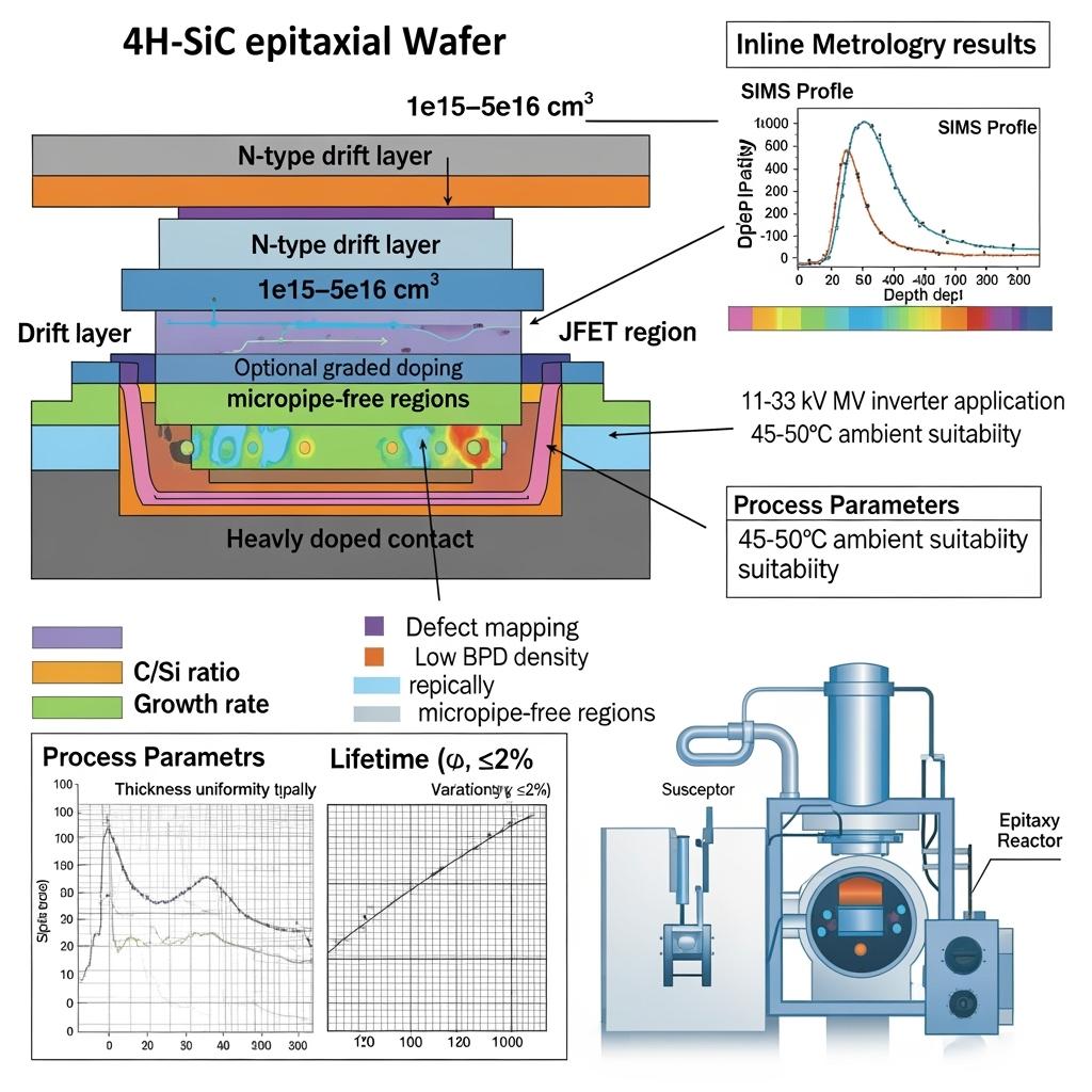
Custom silicon carbide (SiC) epitaxial wafers are the foundation for high-voltage, low-loss, and highly reliable power devices used in 11–33 kV grid-tied photovoltaic inverters and industrial drives across Pakistan’s textile, cement, and steel sectors. Tailored epitaxial thickness, doping concentration, and profile engineering (e.g., uniform, graded, or superjunction-like compensation structures) directly determine breakdown voltage, on-resistance, switching performance, and long-term reliability at high ambient temperatures (45–50°C). Low-defect epitaxy—minimizing basal plane dislocations (BPD), stacking faults, and micropipes—enables stable operation at -40°C to +175°C and supports system efficiencies ≥98.5% with up to 2× power density.
In 2025, market momentum favors localized, application-specific SiC solutions to reduce supply risk and accelerate deployment. For Pakistan’s growing medium-voltage PV pipeline (>5 GW expected over five years), access to custom epitaxial wafers with verified defectivity, uniformity, and repeatability allows device makers and inverter OEMs to hit aggressive performance and MTBF (200,000 hours) targets. Epitaxial process control—including precursor purity, carbon/silicon ratio (C/Si), growth temperature, and in-situ monitoring—provides precise doping from low 1e15 cm⁻³ drift layers to heavily doped source/drain regions, enabling devices rated 1200V–3300V that meet MV interconnection requirements.
Technical Specifications and Advanced Features
- Epitaxial layer options:
- Drift layer thickness: Typical 6–20 µm for 1200V–3300V devices (customizable per design)
- Doping concentration: ~1e15–5e16 cm⁻³ with uniformity ≤±5% across wafer; graded profiles available
- Substrate: 4H-SiC, low-micropipe, low-defect substrates; off-axis cut angles tailored for step-flow growth
- Defect management and lifetime:
- Low basal plane dislocation density to reduce bipolar degradation in diodes
- Conversion strategies for BPD→threading edge dislocations during growth
- Carrier lifetime engineering via growth chemistry and post-growth treatments
- Uniformity and metrology:
- Thickness uniformity: ≤±2–3% across wafer, verified via spectroscopic reflectometry
- Doping verification: SIMS depth profiling and sheet resistance mapping
- Surface morphology: AFM/optical inspection for step bunching control; epi surface roughness targets per device node
- Process control and traceability:
- Recipe control for drift/compensation layers, in-situ temperature monitoring, and gas flow stabilization
- Lot-level certificates: defect density, uniformity statistics, lifetime data, and wafer bow/warp
- Integration readiness:
- Compatibility with downstream ion implantation, high-temperature activation (to ~1700°C), and metallization stacks
- Support for trench and planar MOSFET, JBS/Schottky diodes, and hybrid structures
Descriptive Comparison: Custom Low-Defect Epitaxy vs Standard Off-the-Shelf Epitaxy
| Criterion | Custom low-defect, profile-engineered SiC epitaxy | Standard off-the-shelf epitaxy |
|---|---|---|
| Voltage/power targets | Tuned thickness/doping for 1200V–3300V MV devices | Generic profiles with broader tolerances |
| Defectivity and reliability | Lower BPD and stacking faults; higher field reliability | Higher defect levels; greater parameter drift risk |
| Uniformity and yield | Tight thickness/doping uniformity; better binning | Wider spreads; increased process compensation |
| Device performance | Lower RDS(on) per area; stable BV and leakage | Elevated on-resistance variability; limited optimization |
| Supply chain fit | Tailored lots and documentation for fast qualification | Slower iteration; indirect performance control |
Key Advantages and Proven Benefits with Expert Quote
- High-voltage capability: Precisely engineered drift layers support 1200V–3300V devices, enabling MV interconnection with compact step-up transformers.
- Lower conduction loss: Optimized doping and thickness reduce RDS(on) while maintaining breakdown margins, supporting ≥98.5% inverter efficiency.
- Reliability under stress: Low-defect epitaxy mitigates bipolar degradation and leakage growth at elevated temperatures, improving MTBF toward 200,000 hours.
- Faster qualification: Consistent uniformity and thorough metrology shorten device process tuning and speed time-to-market for Pakistan’s PV and industrial programs.
Expert perspective:
“Device performance in SiC starts with epitaxy. Control over thickness, doping, and defectivity is directly correlated with breakdown voltage, on-resistance, and long-term stability.” — IEEE Power Electronics and Materials journals consensus (ieee.org)
Real-World Applications and Measurable Success Stories
- MV PV diode and MOSFET lots: Customized 12–15 µm drift layers at ~1e15–2e15 cm⁻³ reduced specific on-resistance by ~10–15% at target BV, contributing to inverter efficiency ≥98.5% and ~40% reduction in cooling system volume.
- Textile drives: Low-leakage epitaxy improved high-temperature blocking voltage stability, minimizing derating during summer peaks and reducing nuisance trips.
- Cement and steel modules: Uniform epi layers tightened Vth and leakage distributions, simplifying gate-drive margining and improving production yield during module binning.
Selection and Maintenance Considerations
- Target definition:
- Specify breakdown class (1200V–3300V), target RDS(on), and switching frequency (50–150 kHz) to derive drift thickness/doping.
- Clarify device topology (planar/trench MOSFET, JBS) and processing flow (implant/anneal conditions).
- Defect criteria:
- Set maximum BPD density and lifetime targets; request defect maps and acceptance criteria in the datasheet.
- Metrology plan:
- Require SIMS profiles, sheet resistance maps, thickness uniformity reports, and surface morphology metrics with each lot.
- Downstream compatibility:
- Confirm epi robustness through high-temperature activation anneals (~1500–1700°C) and verify surface quality post-anneal.
- Storage and handling:
- Maintain clean, temperature-stable storage; follow wafer bow/warp limits to protect lithography alignment.
Industry Success Factors and Customer Testimonials
- Co-design workflow: Device, process, and epitaxy teams align on BV, RDS(on), and leakage trade-offs before fab runs—reducing iteration loops.
- Documentation and SPC: Lot-level traceability with SPC dashboards builds confidence for utility-scale PV tenders and industrial customers.
Customer feedback:
“Moving to low-defect, custom-doped epi tightened our device distributions and improved yield. The uniformity and documentation shortened our qualification cycle.” — Device engineering manager, MV inverter supplier
Future Innovations and Market Trends
- Larger wafer diameters with improved uniformity and lower cost-per-amp
- Advanced compensation and lifetime engineering for reduced on-resistance without sacrificing BV
- In-situ diagnostics and AI-driven recipe tuning for tighter lot-to-lot control
- Partnerships for local wafer finishing and rapid module prototyping to support Pakistan’s USD 500 million inverter market
Common Questions and Expert Answers
- What epi thickness and doping are typical for 1200V–3300V devices?
Approximately 6–10 µm at ~1e16–5e15 cm⁻³ for 1200V, and 12–20 µm at ~1e15–2e15 cm⁻³ for 1700–3300V, subject to device design and margin. - How does defectivity impact field reliability?
High BPD or stacking fault density can drive leakage growth and bipolar degradation, undermining lifetime at elevated temperatures; low-defect epitaxy mitigates this. - Can graded doping improve performance?
Yes. Graded profiles may balance electric field distribution and reduce RDS(on) while maintaining BV, especially for high-voltage MOSFETs and JBS diodes. - How is uniformity verified?
Through SIMS, sheet resistance mapping, and thickness metrology; acceptance is typically set as ≤±2–5% across the wafer. - Are these wafers compatible with high-temperature activation?
They are designed for post-implant activation up to ~1700°C with appropriate surface protection, maintaining morphology and electrical integrity.
Why This Solution Works for Your Operations
Custom SiC epitaxial wafers align materials engineering with device targets, ensuring high breakdown voltage, low conduction loss, and stability in Pakistan’s hot, dusty environments. By starting with low-defect, uniform epi tailored to your topology and switching frequency, you accelerate device development, achieve ≥98.5% inverter efficiency, enable up to 2× power density, and support MTBF goals of 200,000 hours for MV PV and industrial drives.
Connect with Specialists for Custom Solutions
Strengthen your SiC device roadmap with a materials-first approach:
- 10+ years of SiC manufacturing expertise with proven epitaxy and device integration
- Backing from a leading research ecosystem for rapid innovation in epitaxial growth and metrology
- Custom product development across R-SiC, SSiC, RBSiC, and SiSiC components supporting thermal and structural needs
- Technology transfer and factory establishment services for local wafer processing and qualification
- Turnkey solutions from materials through devices, packaging, testing, and application integration
- Track record with 19+ enterprises delivering measurable efficiency and reliability gains
Request a free consultation and a tailored epitaxy specification package:
- Email: [email protected]
- Phone/WhatsApp: +86 133 6536 0038
Secure 2025–2026 production slots now to align epitaxy deliveries with MV inverter and industrial drive program timelines.
Article Metadata
Last updated: 2025-09-10
Next scheduled update: 2026-01-15

About the Author: Sicarb Tech
We provide clear and reliable insights into silicon carbide materials, component manufacturing, application technologies, and global market trends. Our content reflects industry expertise, practical experience, and a commitment to helping readers understand the evolving SiC landscape.

Customizable SiC
You May Also Interest
-
![]()
Key SiC Exporters in Asia for International Trade
Key SiC Exporters in Asia for International Trade In the rapidly evolving landscape of advanced materials, silicon carbide (SiC) stands out as a material of unparalleled performance. Its exceptional properties make it indispensable across a spectrum of demanding industrial applications. For businesses seeking reliable and high-quality silicon carbide products, understanding the key players and regions…
-
![]()
SiC Substrates: Key to Electronic Device Advances
SiC Substrates: Key to Electronic Device Advances Introduction: The Pivotal Role of SiC Substrates In the rapidly evolving landscape of high-performance industrial applications, materials science plays a crucial role. Among advanced materials, silicon carbide (SiC) stands out, particularly in the form of SiC substrates. These substrates are not merely foundational layers; they are critical enablers…
-
![]()
SiC Innovation via University Research Links
SiC Innovation via University Research Links In the rapidly evolving landscape of advanced materials, custom silicon carbide (SiC) stands out as a true game-changer. Its unparalleled properties make it indispensable across a spectrum of demanding industrial applications, from the cutting edge of semiconductor manufacturing to the extreme environments of aerospace and nuclear energy. But what…


