Silicon Carbide MOSFET Gate Driver Circuits with dv/dt Control, Short-Circuit Protection, and DESAT Sensing
Share
Product Overview and 2025 Market Relevance
Silicon carbide (SiC) MOSFET gate driver circuits are the control backbone of high-efficiency, high-density power stages. They dictate switching behavior, manage dv/dt and di/dt, and provide critical protection features such as short-circuit shut-down and DESAT sensing. For Pakistan’s textile, cement, and steel sectors—where electrical rooms face 45–50°C ambients and airborne dust—robust gate drivers are essential to achieve ≥98.5% inverter efficiency, up to 2× power density, and long operational life in 11–33 kV distribution-level photovoltaic interconnections and industrial drives.
In 2025, market leaders are aligning gate driver design with SiC device physics: fast Miller plateau transitions, narrow safe operating areas during short-circuit events, and susceptibility to EMI from high dv/dt edges. Application-optimized drivers combine high CMTI (>100 V/ns), precise turn-on/off gate resistors, two-level turn-off (TLO), negative gate bias for immunity, and low-latency DESAT detection. Coupled with isolated power, reinforced digital isolation, and PCB layout rules (Kelvin source, low-inductance loops), these drivers reduce losses, mitigate EMI, and protect modules—even under dust, heat, and grid disturbances common in Pakistan’s industrial environments.
Technical Specifications and Advanced Features
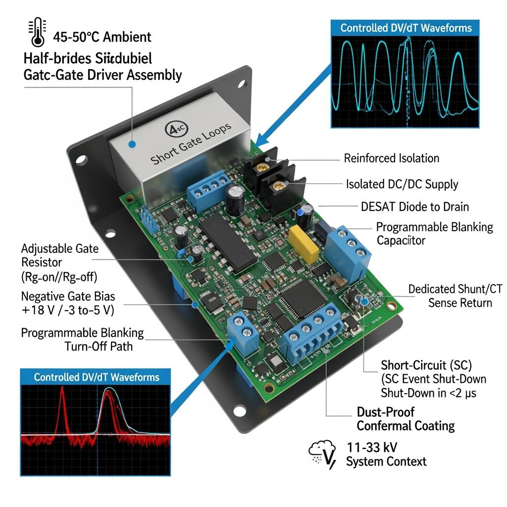
- Drive and isolation
- Gate voltage: +15 to +20 V turn-on; -3 to -5 V turn-off (configurable)
- Peak source/sink current: 6–30 A classes to drive large SiC modules
- Isolation rating: Reinforced insulation for system MV compliance; CMTI ≥ 100 V/ns
- Isolated DC/DC: Low common-mode capacitance, tight regulation, undervoltage lockout (UVLO)
- Switching control
- dv/dt management: Independent Rg_on/Rg_off, optional split-gate drive, and active Miller clamp
- Two-level turn-off (TLO): Soft turn-off path to limit VDS overshoot during fault events
- Slew-rate shaping: Gate current shaping networks to balance loss and EMI
- Protection and diagnostics
- DESAT sensing: Fast short-circuit detection with programmable blanking time and soft-shutdown; <2 µs reaction typical
- Overtemperature input, overcurrent via shunt or Rogowski/CT, and fault latching with fault bus signaling
- Gate monitoring: Open-wire detection, gate-source short detection, and UVLO with deterministic fault handling
- Communications and control
- Interfaces: PWM with deadtime enforcement; optional SPI/UART for telemetry (faults, temperature, event counts)
- Redundant disable lines for safety; watchdog/reset integration
- Environmental and reliability
- Conformal coating options, corrosion-resistant finishes, and extended temperature operation
- Mechanical: Low-inductance gate loop footprints, Kelvin source connectivity, and robust connectors for field service
Descriptive Comparison: SiC-Optimized Gate Drivers vs Conventional IGBT/Silicon Drivers
| Criterion | SiC-optimized gate driver with dv/dt control and DESAT | Conventional IGBT/silicon gate driver |
|---|---|---|
| Switching frequency support | 50–150 kHz with precise dv/dt shaping | 5–20 kHz typical; limited dv/dt control |
| CMTI and EMI robustness | ≥100 V/ns with Miller clamp and negative bias | Lower CMTI; higher susceptibility to false turn-on |
| Short-circuit protection | DESAT with <2 µs reaction and soft shut-down | Slower detection; higher stress during faults |
| Efficiency impact | Lower switching loss, stable operation at high ambient | Higher losses; more derating at temperature |
| Integration with SiC modules | Kelvin source, split gate resistors, fast protection | Often lacks SiC-specific layout and timing |
Key Advantages and Proven Benefits with Expert Quote
- Efficiency and density: dv/dt control and high CMTI enable higher switching frequencies (50–150 kHz), cutting passive size and supporting ≥98.5% efficiency with compact filters and cooling.
- Robust protection: DESAT with TLO prevents catastrophic failures under short-circuit or shoot-through events, reducing downtime and warranty risk.
- EMI-resilient operation: Negative gate bias and Miller clamp mitigate false turn-on, maintaining stability in dusty, hot electrical rooms with long cable harnesses.
- Faster time-to-market: Pre-validated layouts, parameter libraries, and diagnostic telemetry reduce integration effort for 11–33 kV PV and industrial drives.
Expert perspective:
“Gate driver design is pivotal in realizing the advantages of wide bandgap devices; high CMTI isolation, controlled dv/dt, and fast short-circuit protection are indispensable for reliable SiC power stages.” — IEEE Power Electronics Society application guidance (ieee.org)
Real-World Applications and Measurable Success Stories
- Distribution-level PV inverters (southern Pakistan): SiC drivers with DESAT and TLO cut fault-related module damage, while dv/dt shaping yielded THD margin and ≥98.5% efficiency. Systems realized ~40% cooling volume reduction due to stable junction temperatures.
- Textile mill VFDs: Negative bias and split gate resistors eliminated false turn-on during fast transients, reducing nuisance trips and improving loom uptime in 45–50°C ambient conditions.
- Cement and steel drives: Short-circuit ruggedness improved through sub-2 µs DESAT action, reducing IGBT-era protection delays and associated collateral damage. Maintenance calls fell measurably over summer peak loads.
Selection and Maintenance Considerations
- Device pairing
- Match driver current and voltage swing to module gate charge and desired switching speed; ensure Kelvin source availability.
- Validate negative bias level to balance immunity and oxide stress limits.
- Protection tuning
- Set DESAT threshold and blanking time per module characteristics and expected stray inductance.
- Implement TLO resistor sizing to limit VDS overshoot without prolonging energy dissipation.
- PCB/layout
- Minimize loop inductance; segregate power and logic grounds; use dedicated return for DESAT and sense lines.
- Place DC/DC and isolator away from high di/dt nodes; enforce creepage/clearance appropriate for MV systems.
- Environmental hardening
- Apply conformal coating for dust; specify high-temperature components; verify operation at 45–50°C ambient.
- Verification
- Conduct double-pulse tests to tune dv/dt; short-circuit tests to validate TSC reaction; EMC pre-compliance for conducted/radiated emissions.
Industry Success Factors and Customer Testimonials
- Co-design with module packaging and LCL filter teams aligns dv/dt targets with EMI and THD goals, cutting redesign loops.
- Early mission-profile validation reduces over-engineering and cost while maintaining reliability.
Customer feedback:
“Integrating fast DESAT and two-level turn-off into our SiC half-bridges eliminated field failures from rare short-circuit events. dv/dt tuning improved EMI headroom without sacrificing efficiency.” — Lead power engineer, C&I PV integrator in Sindh
Future Innovations and Market Trends
- Digital gate drivers with adaptive dv/dt control based on real-time current and temperature sensing
- Integrated condition monitoring (SOH metrics) for gate charge and threshold drift tracking
- Higher CMTI isolation technologies and lower common-mode capacitance for multi-MW MV systems
- Reference designs tailored for Pakistan’s MV PV pipeline (>5 GW) with local manufacturing support
Common Questions and Expert Answers
- Why use negative gate bias with SiC MOSFETs?
To prevent false turn-on from Miller coupling at high dv/dt. Typical values are -3 to -5 V, selected per device limits and EMI targets. - How fast should DESAT protection be?
Target total reaction times under ~2 µs from fault onset to current interruption, with soft-shutdown to limit overvoltage stress. - What is two-level turn-off and why use it?
TLO introduces a controlled, softer turn-off during faults to reduce VDS overshoot and stray inductive ringing, protecting the module and gate oxide. - How do I tune dv/dt without losing efficiency?
Use split Rg_on/Rg_off, layout to reduce inductance, and optionally gate current shaping; iterate via double-pulse testing to balance EMI and switching loss. - Can these drivers operate reliably at 45–50°C with dust?
Yes. With conformal coating, derated components, and proper airflow or sealing, drivers maintain stability and protection performance.
Why This Solution Works for Your Operations
These SiC-focused gate driver circuits deliver the control precision and protection speed required for Pakistan’s MV interconnections and heavy-duty industrial drives. They enable higher switching frequencies for compact LCL filters, stabilize operation in hot, dusty environments, and guard against damaging faults—unlocking ≥98.5% efficiency, up to 2× power density, and long service life across textile, cement, and steel applications.
Connect with Specialists for Custom Solutions
Accelerate your SiC power stage with expert driver design and validation:
- 10+ years of SiC manufacturing expertise and application engineering
- Backing from a leading research ecosystem driving innovation in isolation, protection, and EMI control
- Custom product development across R-SiC, SSiC, RBSiC, and SiSiC components influencing thermal and mechanical reliability
- Technology transfer and factory establishment services for local driver assembly and testing
- Turnkey solutions from devices and drivers to filters, cooling, and compliance
- Proven results with 19+ enterprises delivering efficiency, reliability, and faster time-to-market
Request a free consultation and a tailored gate driver specification package:
- Email: [email protected]
- Phone/WhatsApp: +86 133 6536 0038
Book your 2025–2026 development slots now to secure co-design, EMC validation, and field pilots aligned with MV PV and industrial drive rollouts.
Article Metadata
Last updated: 2025-09-10
Next scheduled update: 2026-01-15

About the Author: Sicarb Tech
We provide clear and reliable insights into silicon carbide materials, component manufacturing, application technologies, and global market trends. Our content reflects industry expertise, practical experience, and a commitment to helping readers understand the evolving SiC landscape.

Customizable SiC
You May Also Interest
-
![]()
SiC Substrates: Key to Electronic Device Advances
SiC Substrates: Key to Electronic Device Advances Introduction: The Pivotal Role of SiC Substrates In the rapidly evolving landscape of high-performance industrial applications, materials science plays a crucial role. Among advanced materials, silicon carbide (SiC) stands out, particularly in the form of SiC substrates. These substrates are not merely foundational layers; they are critical enablers…
-
![]()
SiC Innovation via University Research Links
SiC Innovation via University Research Links In the rapidly evolving landscape of advanced materials, custom silicon carbide (SiC) stands out as a true game-changer. Its unparalleled properties make it indispensable across a spectrum of demanding industrial applications, from the cutting edge of semiconductor manufacturing to the extreme environments of aerospace and nuclear energy. But what…
-
![]()
Next-Gen SiC Wafers for Power Electronics Excellence
Next-Gen SiC Wafers for Power Electronics Excellence Introduction: The Pivotal Role of SiC Wafers in Modern Power Electronics The relentless pursuit of higher efficiency, increased power density, and superior performance in power electronic systems has spotlighted silicon carbide (SiC) as a transformative material. SiC wafers, the foundational substrates for SiC-based power devices, are at the…