SiC in Telecom: Enabling Faster, More Reliable Networks
Share
SiC in Telecom: Enabling Faster, More Reliable Networks
Introduction: The Pivotal Role of Custom Silicon Carbide in Modern Telecommunications
The telecommunications industry is undergoing an unprecedented transformation, driven by the insatiable demand for higher data rates, lower latency, and ubiquitous connectivity. Technologies like 5G, the Internet of Things (IoT), and advanced satellite communications are pushing the boundaries of existing materials and components. In this high-stakes environment, custom silicon carbide (SiC) products are emerging as critical enablers. Silicon carbide, a compound of silicon and carbon, is a high-performance technical ceramic renowned for its exceptional thermal, electrical, and mechanical properties. Unlike traditional semiconductor materials like silicon, SiC offers superior performance in high-power, high-frequency, and high-temperature applications, making it indispensable for the next generation of telecom infrastructure. The ability to customize SiC components allows engineers to precisely meet the stringent demands of advanced telecom systems, ensuring optimal performance, reliability, and efficiency. From base stations to optical networks and satellite payloads, custom SiC is laying the foundation for a faster, more connected world.
The quest for enhanced network performance necessitates materials that can handle increased power densities, operate at higher frequencies, and withstand harsh environmental conditions. Silicon carbide technical ceramics provide a robust solution, offering a unique combination of properties such as high thermal conductivity, wide bandgap, high breakdown electric field, and excellent chemical inertness. These characteristics translate directly into tangible benefits for telecom applications, including more efficient power conversion, reduced signal loss, smaller component sizes, and improved system longevity. As network complexity grows, the importance of reliable, high-performance materials like SiC cannot be overstated.
Main Applications of SiC in Telecommunications
The versatility of silicon carbide allows its application across a wide spectrum of telecommunication systems. Its unique properties address key challenges in signal amplification, power management, thermal control, and component durability.
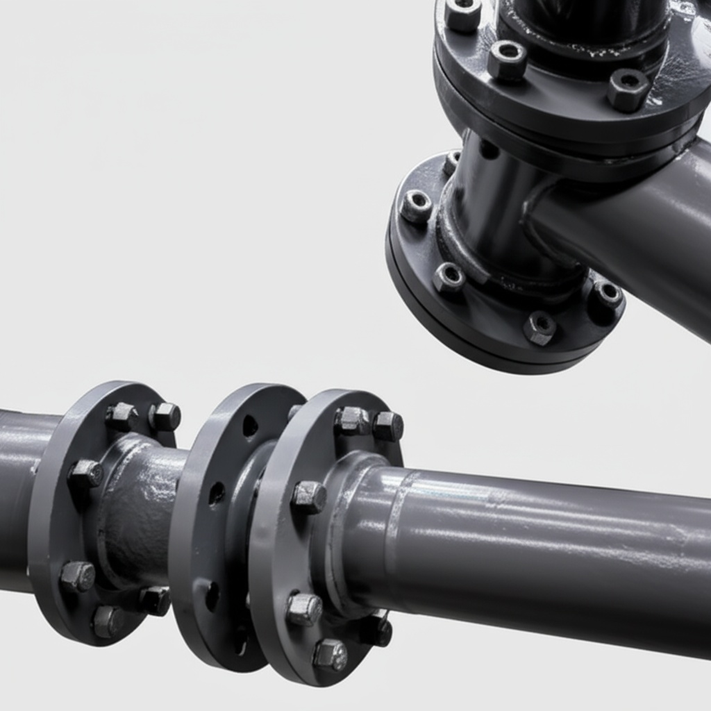
- Radio Frequency (RF) Applications: SiC is increasingly used in high-power RF devices such as transistors (e.g., GaN-on-SiC HEMTs), filters, and resonators. Its high thermal conductivity allows for efficient heat dissipation, critical for maintaining performance and reliability in powerful RF amplifiers used in base stations and satellite communication systems. SiC substrates for GaN RF devices are particularly vital for 5G infrastructure.
- Power Electronics: Telecom power supplies, inverters, and converters benefit immensely from SiC-based diodes and MOSFETs. These devices offer higher switching frequencies, lower losses, and higher operating temperatures compared to their silicon counterparts, leading to more compact, efficient, and reliable power systems for base stations, data centers, and network equipment.
- Optical Networking: In fiber optic communication, precision SiC components can be used for mounts, benches, and structural elements where thermal stability and stiffness are paramount. Custom SiC components ensure alignment accuracy of optical elements over varying temperatures.
- Thermal Management Solutions: The exceptional thermal conductivity of SiC (often exceeding 200 W/mK for specialized grades) makes it an ideal material for SiC heat sinks, heat spreaders, and thermal management components in densely packed telecom equipment. Effective heat dissipation is crucial for component longevity and stable operation.
- Microwave and Millimeter-Wave Components: At higher frequencies (microwave and millimeter-wave bands) used in 5G and beyond, SiC’s low dielectric loss and high power handling capability are advantageous for waveguides, antennas, and other passive components.
- Satellite Communications: Components in satellites are exposed to extreme temperature fluctuations and radiation. SiC’s thermal stability, radiation resistance, and lightweight nature (compared to some traditional metals) make it suitable for structural parts, mirrors, and electronic packaging in satellite payloads.
- Test and Measurement Equipment: High-precision SiC components are also used in equipment designed to test telecom devices, where dimensional stability and wear resistance are crucial for accurate and repeatable measurements.
Why Choose Custom Silicon Carbide for Telecom Networks?
The decision to opt for custom silicon carbide components in telecommunication networks is driven by a compelling set of advantages that directly address the industry’s evolving needs for higher performance, reliability, and efficiency.
- Enhanced Thermal Management: Telecom equipment, especially 5G base stations and high-power amplifiers, generates significant heat. SiC’s high thermal conductivity allows for superior heat dissipation, preventing overheating, improving device longevity, and enabling more compact designs. Custom designs can optimize heat paths for specific applications.
- Superior High-Frequency Performance: SiC’s wide bandgap and high electron saturation velocity enable devices to operate efficiently at higher frequencies with lower losses. This is critical for 5G, millimeter-wave applications, and next-generation wireless technologies. Custom SiC substrates can be tailored for optimal RF performance.
- Increased Power Density: SiC devices can handle higher voltages and currents in smaller packages compared to silicon. This leads to increased power density, allowing for smaller and lighter telecom equipment without sacrificing power output. This is particularly beneficial for pole-mounted 5G small cells and satellite payloads.
- Improved Durability and Reliability: SiC exhibits excellent mechanical strength, hardness, and resistance to wear and erosion. This makes durable SiC components ideal for telecom infrastructure deployed in harsh outdoor environments or applications involving physical movement. Its chemical inertness also protects against corrosion.
- Miniaturization: The superior properties of SiC allow for the design of smaller and lighter components. Customization enables integration of multiple functions into single SiC parts, further contributing to system miniaturization, a key trend in modern telecom hardware.
- Reduced System-Level Costs: While SiC components may have a higher initial cost, their superior efficiency, reliability, and longevity can lead to lower overall system-level costs. This includes reduced energy consumption, lower cooling requirements, and less frequent maintenance or replacement.
- Tailored Solutions for Specific Needs: Telecom applications are diverse, each with unique requirements. Custom SiC manufacturing allows for the creation of components with specific geometries, surface finishes, and material compositions, perfectly aligning with the intended application, from RF filters to power module substrates.
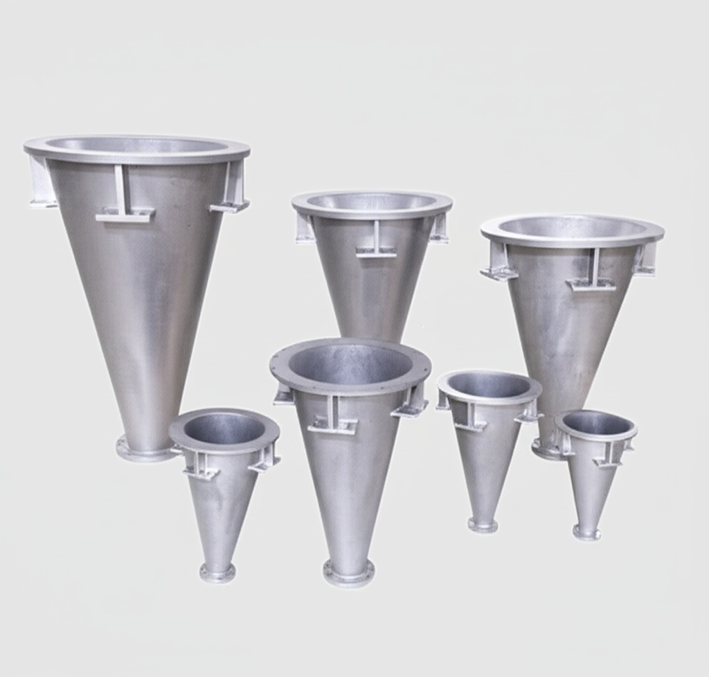
Recommended SiC Grades and Compositions for Telecom Components
The choice of silicon carbide grade is critical for optimizing performance in specific telecommunication applications. Different manufacturing processes yield SiC materials with varying properties. Key grades relevant to the telecom sector include:
| SiC Grade | Key Characteristics | Typical Telecom Applications |
|---|---|---|
| Sintered Silicon Carbide (SSiC) | High purity (typically >99%), excellent chemical resistance, high strength and hardness, good thermal conductivity (150-250 W/mK), good wear resistance. | Structural components, heat sinks, substrates for power electronics, components for harsh environments, precision alignment fixtures. |
| Reaction-Bonded Silicon Carbide (RBSiC or SiSiC) | Contains some free silicon (typically 8-15%), good thermal conductivity (120-180 W/mK), excellent thermal shock resistance, relatively easier to form complex shapes, good dimensional stability. | Heat spreaders, larger structural components, RF filters, antenna components where extreme purity is not the primary concern but thermal performance and complex geometry are. |
| Chemical Vapor Deposited SiC (CVD-SiC) | Ultra-high purity (>99.999%), exceptional thermal conductivity (can exceed 300 W/mK for specific forms like isotopic SiC), excellent surface finish capabilities, superior dielectric properties. | High-performance substrates for RF and microwave devices, optical components, semiconductor processing equipment used to make telecom chips. Often more expensive. |
| Nitride-Bonded Silicon Carbide (NBSiC) | Good thermal shock resistance, high hot strength, good resistance to abrasion. Often used in more rugged industrial applications but can find uses in support structures. | Support structures in manufacturing processes for telecom components, specialized fixtures. |
| Porous SiC | Controlled porosity, lightweight, good for filtration or as a core material for composites. Specific grades can offer tailored thermal or dielectric properties. | Specialized RF absorbers, lightweight structural supports, wicking structures for heat pipes in telecom cooling systems. |
The selection process involves a trade-off between desired properties (e.g., thermal conductivity, electrical resistivity, mechanical strength), manufacturability of complex shapes, and cost. For instance, while CVD-SiC offers the highest purity and thermal conductivity, SSiC or RBSiC might provide a more cost-effective solution for applications where these ultra-high-end properties are not strictly necessary but still demand performance beyond traditional materials. High-purity SiC grades are often preferred for applications directly in the signal path or requiring specific dielectric properties, while grades like RBSiC are excellent for thermal management components where a balance of performance and cost is crucial.
Design Considerations for SiC Products in Telecom Infrastructure
Designing components with silicon carbide for telecommunications infrastructure requires careful consideration of its unique material properties and manufacturing processes to ensure optimal performance, reliability, and cost-effectiveness.
- Thermal Management Integration: Given SiC’s excellent thermal conductivity, designs should maximize heat dissipation paths. This includes optimizing the geometry of SiC heat sinks, ensuring good thermal contact with heat-generating devices, and considering airflow or liquid cooling integration. Finite Element Analysis (FEA) for thermal simulation is highly recommended.
- High-Frequency Electrical Performance: For RF and microwave applications, design aspects such as dielectric constant, loss tangent, surface roughness, and metallization compatibility of the SiC material are critical. The geometry of SiC substrates and waveguides must be precisely controlled to achieve desired impedance and minimize signal loss. Custom precision SiC manufacturing is key here.
- Managing Brittleness: SiC is a hard but brittle ceramic. Designs should avoid sharp corners, stress concentrations, and thin, unsupported sections. Generous radii, chamfers, and robust support structures are advisable. Consideration must be given to impact resistance and handling during assembly and maintenance.
- Machinability and Complexity: While SiC can be machined to tight tolerances, it is a hard material, making machining complex and costly. Designs should aim for simplicity where possible. Features like blind holes, deep pockets, and complex curvatures will increase manufacturing time and cost. Discussing design for manufacturability (DfM) with the SiC supplier is crucial.
- Joining and Assembly: Consider how SiC components will be integrated into larger assemblies. Methods like brazing, diffusion bonding, or mechanical clamping are used. The choice of joining method can affect the overall design and thermal expansion compatibility with adjoining materials.
- Metallization: For many electronic applications, SiC components require metallization for electrical contacts or brazing. The type of metallization (e.g., Ti/Pt/Au, Ni) and its adhesion strength are important design considerations, particularly for reliability under thermal cycling.
- Miniaturization and Integration: Leveraging SiC’s properties can lead to smaller components. Designers should explore possibilities for integrating multiple functions into a single custom SiC part to reduce system size, weight, and part count.
- Environmental Factors: While SiC is generally robust, specific telecom environments (e.g., coastal areas with salt spray, extreme temperatures in outdoor base stations, vacuum in space for satellite components) should be considered in material grade selection and protective coatings if necessary.
Effective design is a collaborative process between the telecom engineer and the SiC component manufacturer. Early engagement ensures that the design is optimized for both performance and manufacturability.
Tolerance, Surface Finish & Dimensional Accuracy for Telecom SiC Parts
In the demanding world of telecommunications, the precision of components is paramount. For silicon carbide parts used in telecom systems, achieving tight tolerances, specific surface finishes, and high dimensional accuracy is critical for ensuring optimal performance, interoperability, and reliability.
Tolerances:
Silicon carbide, being a very hard material, requires specialized grinding and machining processes to achieve precise dimensions. Typical achievable tolerances for SiC components depend on the size and complexity of the part, as well as the specific SiC grade and manufacturing method (e.g., sintered vs. reaction-bonded).
- Standard Tolerances: For general features, tolerances can range from ±0.1 mm to ±0.5 mm.
- Precision Tolerances: With advanced grinding and lapping techniques, it’s possible to achieve much tighter tolerances, often in the range of ±0.005 mm to ±0.025 mm (±5 to 25 microns) for critical dimensions, flatness, and parallelism.
- Impact on Cost: Tighter tolerances invariably lead to increased manufacturing costs due to more complex machining operations, higher tooling wear, and increased inspection time. It’s essential to specify only the necessary level of precision for each feature to manage costs effectively.
Surface Finish:
The surface finish of SiC components is crucial for various telecom applications:
- RF and Microwave Applications: Smooth surfaces (low Ra values) are necessary for substrates and waveguides to minimize signal loss at high frequencies. Surface roughness can impact conductor losses and overall device efficiency. Finishes with Ra < 0.1 µm are often required.
- Optical Components: For SiC mirrors or benches in optical communication systems, exceptionally smooth and polished surfaces (Ra in the nanometer range) are needed to achieve desired reflectivity and minimize light scattering.
- Sealing Surfaces: Components that require hermetic sealing or precise mating with other parts need controlled surface finishes to ensure a proper seal or interface.
- Achievable Finishes:
- As-fired: Surface finish can be rougher, suitable for non-critical surfaces.
- Ground: Ra values typically range from 0.4 µm to 1.6 µm.
- Lapped/Polished: Ra values can be brought down to < 0.05 µm, or even to angstrom levels for super-polished surfaces.
Dimensional Accuracy:
Dimensional accuracy refers to the conformity of the manufactured part to the specified dimensions in the engineering drawing. For SiC components in telecom, this includes:
- Geometric Dimensioning and Tolerancing (GD&T): Features like flatness, parallelism, perpendicularity, and circularity are often critical and must be tightly controlled, especially for mounting surfaces, interfaces, and components in resonant structures.
- Consistency: High dimensional accuracy ensures part-to-part consistency, which is vital for automated assembly processes and predictable system performance.
Achieving the required tolerances, surface finishes, and dimensional accuracy for telecom SiC parts necessitates advanced manufacturing capabilities, including precision diamond grinding, lapping, polishing machines, and sophisticated metrology equipment (e.g., CMMs, optical profilometers, interferometers). Close collaboration with a supplier experienced in precision SiC machining is essential.
Post-Processing Needs for SiC in Telecommunication Systems
After the initial forming and sintering (or reaction bonding) of silicon carbide components, various post-processing steps are often necessary to meet the stringent requirements of telecommunication applications. These steps refine the component’s geometry, surface characteristics, and functionality.
- Grinding: As SiC is extremely hard, diamond grinding is the primary method for achieving precise dimensions and tolerances. This can include surface grinding for flatness, cylindrical grinding for rods and tubes, and complex profile grinding for intricate shapes. Precision diamond grinding is fundamental for most telecom SiC parts.
- Lapping and Polishing: For applications requiring ultra-smooth surfaces, such as RF substrates, optical components, or sealing surfaces, lapping and polishing are employed. These processes use progressively finer abrasive slurries to achieve low Ra values and mirror-like finishes. This is critical for minimizing signal loss at high frequencies or ensuring optical performance.
- Machining of Features: Creating holes, threads (though challenging and often avoided if possible), slots, and other specific features may require specialized diamond tooling and CNC machining techniques. Electrical Discharge Machining (EDM) can sometimes be used for complex shapes in certain SiC grades, though it’s less common than grinding.
- Cleaning: Thorough cleaning is essential to remove any contaminants, machining oils, or particulate matter from the manufacturing process. Multi-stage ultrasonic cleaning processes with specialized detergents and deionized water are common, especially for high-purity applications.
- Edge Chamfering/Radiusing: To reduce the risk of chipping on brittle SiC components and to improve handling safety, edges are often chamfered or radiused. This can also reduce stress concentrations.
- Metallization: For many electronic and some joining applications, SiC surfaces need to be metallized. This involves depositing thin layers of metal (e.g., Ti, Pt, Au, Ni, W) through processes like sputtering or evaporation. Metallization provides conductive paths, contact pads for wire bonding, or surfaces for brazing. Adhesion strength and uniformity of the metallization layer are critical.
- Coatings: In some specific telecom scenarios, specialized coatings might be applied to SiC components to enhance certain properties. For example, anti-reflective coatings for optical applications or protective coatings for extremely corrosive environments (though SiC itself is highly resistant).
- Annealing: Stress relief annealing may sometimes be performed after extensive machining to mitigate any internal stresses introduced during the process, enhancing the component’s long-term stability and strength.
- Inspection and Metrology: While not a processing step itself, rigorous inspection using CMMs, optical profilometers, SEM, and other advanced metrology tools is a crucial part of the post-processing workflow to ensure all specifications are met.
The extent and type of post-processing depend heavily on the specific telecom application and the required performance characteristics of the custom SiC component. Each step adds to the cost and lead time, so they should be specified based on genuine functional requirements.
Common Challenges in Utilizing SiC for Telecom and How to Overcome Them
While silicon carbide offers significant advantages for telecommunication applications, engineers and procurement managers should be aware of potential challenges. Understanding these challenges and their mitigation strategies is key to successful SiC implementation.
| Challenge | Description | Mitigation Strategies |
|---|---|---|
| Brittleness and Fracture Toughness | SiC is a ceramic material and is inherently brittle, meaning it has low fracture toughness compared to metals. This can lead to chipping or catastrophic failure under impact or high tensile stress. |
|
| Machining Complexity and Cost | Due to its extreme hardness, machining SiC is difficult, time-consuming, and requires specialized diamond tooling. This can lead to higher manufacturing costs compared to conventional materials. |
|
| Thermal Expansion Mismatch | When SiC is joined to other materials (e.g., metals in a package), differences in coefficients of thermal expansion (CTE) can induce stress during temperature cycling, potentially leading to joint failure or SiC fracture. |
|
| Material Purity and Consistency | For certain high-frequency or semiconductor-grade applications, impurities or inconsistencies in SiC material can degrade performance. |
|
| Joining and Metallization Challenges | Achieving strong, reliable, and hermetic bonds between SiC and other materials, or creating adherent and stable metallization layers, can be complex. |
|
| Cost of Raw Materials and Processing | High-purity SiC powders and specialized manufacturing processes contribute to a higher material and component cost compared to traditional ceramics or metals. |
|
Overcoming these challenges often involves a close collaboration between the end-user and an experienced custom silicon carbide solutions provider. Early engagement in the design phase can help anticipate and mitigate many of these potential issues, ensuring the successful deployment of SiC components in demanding telecom applications.
How to Choose the Right SiC Supplier for Your Telecom Needs
Selecting the right silicon carbide supplier is a critical decision that can significantly impact the quality, performance, and cost-effectiveness of your telecommunication components. The ideal partner will offer more than just manufacturing; they will provide expertise, support, and reliability.
- Technical Expertise and Experience: Look for a supplier with a deep understanding of silicon carbide materials science, manufacturing processes, and the specific demands of telecom applications. They should be able to advise on material selection, design optimization, and potential challenges. Experience with high-frequency SiC applications or thermal management solutions is a plus.
- Customization Capabilities: Telecom systems often require highly specialized components. Ensure the supplier has robust capabilities for custom SiC product manufacturing, including complex geometries, tight tolerances, and specific surface finishes.
- Material Quality and Variety: A good supplier should offer a range of SiC grades (RBSiC, SSiC, etc.) and be transparent about material properties and sourcing. They should have stringent quality control measures for raw materials and throughout the manufacturing process.
- Manufacturing Capabilities and Technology: Assess their manufacturing facility, equipment (e.g., for pressing, sintering, grinding, lapping, metrology), and technological sophistication. Do they invest in modern technology to ensure precision and efficiency?
- Quality Management Systems: Certifications like ISO 9001 demonstrate a commitment to quality. Inquire about their quality assurance procedures, inspection protocols, and material traceability.
- Design and Engineering Support: Value-added services like DfM (Design for Manufacturability) support, FEA (Finite Element Analysis) for thermal or mechanical simulation, and prototyping services can be invaluable.
- Supply Chain Reliability and Location: Consider the supplier’s location, lead times, and ability to ensure a stable supply. For instance, the city of Weifang in China has emerged as a significant hub of China’s silicon carbide customizable parts factories. This region hosts over 40 SiC production enterprises, accounting for more than 80% of China’s total SiC output.
- Introducing Sicarb Tech:Within this vital hub, our company, Sicarb Tech, stands out. Since 2015, we have been instrumental in advancing silicon carbide production technology, supporting local enterprises in achieving large-scale production and significant product process improvements. We are proud to have witnessed and contributed to the growth of this vibrant SiC industry cluster.

About the Author: Sicarb Tech
We provide clear and reliable insights into silicon carbide materials, component manufacturing, application technologies, and global market trends. Our content reflects industry expertise, practical experience, and a commitment to helping readers understand the evolving SiC landscape.

Customizable SiC
You May Also Interest
-
![]()
SiC Substrates: Key to Electronic Device Advances
SiC Substrates: Key to Electronic Device Advances Introduction: The Pivotal Role of SiC Substrates In the rapidly evolving landscape of high-performance industrial applications, materials science plays a crucial role. Among advanced materials, silicon carbide (SiC) stands out, particularly in the form of SiC substrates. These substrates are not merely foundational layers; they are critical enablers…
-
![]()
SiC Innovation via University Research Links
SiC Innovation via University Research Links In the rapidly evolving landscape of advanced materials, custom silicon carbide (SiC) stands out as a true game-changer. Its unparalleled properties make it indispensable across a spectrum of demanding industrial applications, from the cutting edge of semiconductor manufacturing to the extreme environments of aerospace and nuclear energy. But what…
-
![]()
Next-Gen SiC Wafers for Power Electronics Excellence
Next-Gen SiC Wafers for Power Electronics Excellence Introduction: The Pivotal Role of SiC Wafers in Modern Power Electronics The relentless pursuit of higher efficiency, increased power density, and superior performance in power electronic systems has spotlighted silicon carbide (SiC) as a transformative material. SiC wafers, the foundational substrates for SiC-based power devices, are at the…