SiC: Accelerating EV Application Growth & Efficiency

Share
SiC: Accelerating EV Application Growth & Efficiency
The automotive industry is undergoing a monumental shift towards electrification, driven by consumer demand, regulatory pressures, and technological advancements. At the heart of this transformation lies the pursuit of greater efficiency, longer range, faster charging, and enhanced performance in electric vehicles (EVs). Silicon Carbide (SiC), an advanced semiconductor material, is rapidly emerging as a cornerstone technology enabling these advancements. This blog post delves into the critical role of custom silicon carbide products in accelerating EV application growth and efficiency, offering insights for engineers, procurement managers, and technical buyers across the automotive and related sectors.
The EV Revolution: Why Silicon Carbide is a Game Changer
Electric vehicles demand power electronics that can operate at higher voltages, temperatures, and frequencies compared to traditional internal combustion engine vehicles. Silicon (Si), the incumbent semiconductor material, is reaching its theoretical limits in meeting these increasingly stringent requirements. Silicon Carbide, with its superior material properties, offers a significant leap forward. Its wider bandgap, higher thermal conductivity, and greater critical electric field strength translate directly into tangible benefits for EV systems, making it indispensable for next-generation electric mobility.
- Higher Efficiency: SiC devices exhibit lower switching and conduction losses, leading to improved overall powertrain efficiency.
- Increased Power Density: The ability to operate at higher temperatures and frequencies allows for smaller, lighter components, increasing power density.
- Enhanced Thermal Management: Superior thermal conductivity simplifies cooling requirements, reducing system complexity and weight.
- Faster Switching Speeds: SiC enables higher switching frequencies, which can reduce the size of passive components like inductors and capacitors.
Key EV Applications Driving Demand for SiC Technology
Silicon Carbide is finding widespread adoption across various critical systems within electric vehicles. Its unique properties are particularly beneficial in applications where power conversion efficiency and thermal performance are paramount.
| EV Application | Benefit of SiC Integration | Impact on EV Performance |
|---|---|---|
| Main Inverters | Higher efficiency, reduced switching losses, higher operating temperature. | Increased vehicle range, improved acceleration, smaller inverter size and weight. |
| On-Board Chargers (OBCs) | Faster charging times, higher efficiency, increased power density. | Reduced charging duration, more compact and lighter OBC units. |
| DC-DC Converters | Higher efficiency in converting high voltage battery power to lower voltage for auxiliary systems. | Improved overall energy management, reduced size of converters. |
| Electric Compressors (e.g., for A/C) | More efficient operation, reduced energy consumption from the battery. | Longer range by minimizing auxiliary load, improved climate control performance. |
| Fast Charging Infrastructure | Enables higher power delivery, improved thermal management in charging stations. | Significantly reduced charging times for EV users, more robust charging stations. |
The integration of SiC in these applications is not just an incremental improvement but a transformative step, paving the way for EVs that are more practical, powerful, and aligned with consumer expectations for range and charging convenience.
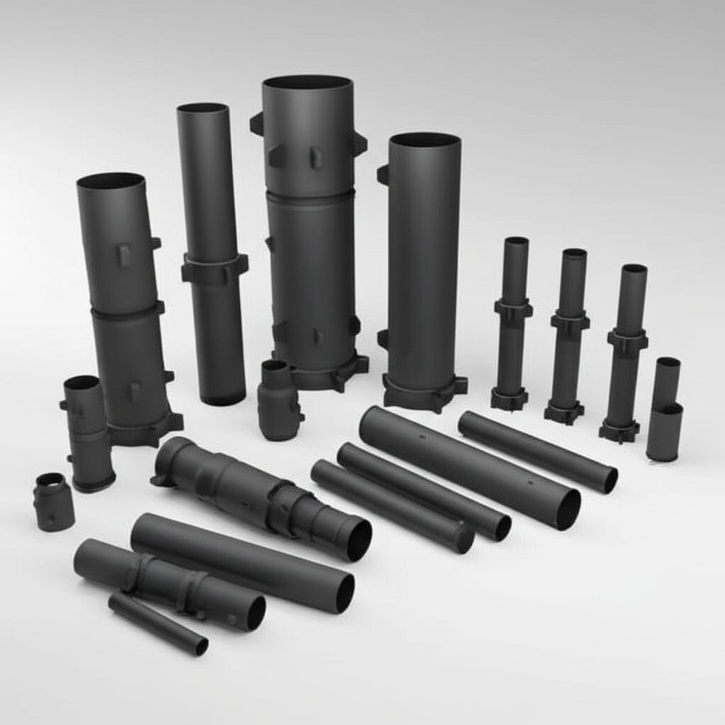
Advantages of Custom Silicon Carbide Components for EV Manufacturers
While off-the-shelf SiC components offer benefits, custom silicon carbide solutions provide EV manufacturers with a distinct competitive edge. Tailoring SiC components to specific application requirements allows for optimization of performance, form factor, and integration within complex EV architectures.
- Optimized Performance: Custom designs can fine-tune electrical and thermal characteristics to match the precise needs of a particular EV system, maximizing efficiency and reliability.
- Enhanced Thermal Management: Custom geometries and packaging can improve heat dissipation, crucial for high-power EV applications like inverters and chargers. This might involve specific mounting features or integrated cooling channels.
- Improved Power Density: Tailored form factors allow for more compact and lightweight designs, contributing to overall vehicle weight reduction and increased space for other components or passenger comfort.
- Application-Specific Integration: Custom SiC modules can be designed for seamless integration into existing or new EV platforms, reducing assembly time and complexity.
- Durability and Reliability: Components can be designed to withstand specific mechanical stresses, vibrations, and environmental conditions encountered in automotive use, enhancing long-term reliability. For instance, customized mechanical supports or encapsulation can be incorporated.
- Supply Chain Security: Partnering with a specialized custom SiC provider can offer a more stable and tailored supply chain, crucial for high-volume automotive production.
Investing in custom SiC solutions allows OEMs to push the boundaries of EV performance and differentiate their offerings in a rapidly growing market.
Recommended Silicon Carbide Grades for Demanding EV Environments
The choice of SiC grade is critical for ensuring optimal performance and longevity in the harsh operating conditions of electric vehicles. Different manufacturing processes yield SiC materials with varying properties. For EV applications, grades that offer high purity, excellent thermal conductivity, and robust mechanical strength are preferred.
Common types of SiC relevant to EV applications include:
- Sintered Silicon Carbide (SSC): Produced by sintering SiC powder at high temperatures (often >2000°C).
- Properties: High density, excellent strength, high thermal conductivity, superior wear and corrosion resistance.
- EV Relevance: Ideal for structural components requiring high strength and thermal stability, such as substrates for power modules, heat sinks, and wear-resistant parts in pumps or compressors.
- Reaction-Bonded Silicon Carbide (RBSC or SiSiC): Manufactured by infiltrating a porous carbon preform with molten silicon. The silicon reacts with some of the carbon to form SiC, and the remaining pores are filled with silicon metal.
- Properties: Good mechanical strength, excellent thermal shock resistance, high thermal conductivity, relatively easier to produce complex shapes.
- EV Relevance: Suitable for components where complex geometries are needed alongside good thermal performance, such as heat exchanger elements or specific types of power electronic module packaging.
- Chemical Vapor Deposited (CVD) SiC: A high-purity form of SiC produced by chemical vapor deposition processes.
- Properties: Extremely high purity, excellent surface finish, superior chemical resistance, and often used for SiC epitaxial layers on SiC substrates for active device fabrication.
- EV Relevance: Primarily for the SiC wafers and epitaxial layers used in manufacturing SiC MOSFETs and diodes – the core of SiC power devices. Custom structural components made from CVD SiC can also be used where extreme purity or specific surface properties are paramount.
- Nitride-Bonded Silicon Carbide (NBSC): SiC grains bonded by a silicon nitride phase.
- Properties: Good thermal shock resistance, moderate strength, good resistance to molten metals.
- EV Relevance: Less common in direct power electronics but might find use in auxiliary high-temperature components or manufacturing equipment for EV parts.
For EV power modules and inverters, high-purity sintered SiC substrates and CVD-grown SiC epitaxial layers are particularly crucial. The choice often depends on the specific balance of thermal, electrical, mechanical, and cost requirements of the application.
Critical Design Considerations for SiC in EV Systems
Successfully integrating SiC components into EV systems requires careful design considerations to fully leverage their benefits while mitigating potential challenges. Engineers must account for the unique properties of SiC compared to traditional silicon.
- Thermal Management Strategy:
- While SiC has high thermal conductivity, the increased power density means effective heat dissipation is still critical. Custom heat sink designs, advanced cooling techniques (liquid cooling, phase change materials), and optimized thermal interfaces are essential.
- Consider CTE (Coefficient of Thermal Expansion) mismatches between SiC and surrounding materials (e.g., copper baseplates, PCBs) to prevent stress and delamination over temperature cycles.
- Electrical Layout and Parasitics:
- SiC devices can switch at very high speeds. This necessitates minimizing parasitic inductance and capacitance in the circuit layout to reduce ringing, overshoot, and EMI (Electromagnetic Interference).
- Shorter, wider traces, careful component placement, and laminated bus bar designs are often employed.
- Gate Drive Design:
- SiC MOSFETs have different gate drive requirements compared to Si IGBTs (e.g., recommended gate voltages, need for negative turn-off voltage for some devices).
- Robust gate driver circuits capable of providing fast, clean gate signals are crucial for optimal switching performance and reliability.
- Mechanical Integrity and Packaging:
- SiC is a brittle ceramic material. Mechanical stress due to vibration, shock, or CTE mismatch must be carefully managed through appropriate packaging and mounting techniques.
- Advanced packaging solutions, such as sinter-joining for die attach and advanced wire bonding or copper clip technologies, are used to improve reliability and thermal performance.
- Cost vs. Performance Trade-offs:
- While SiC offers superior performance, it is currently more expensive than silicon. Designers must evaluate the system-level benefits (e.g., reduced cooling needs, smaller passives, improved efficiency) to justify the component cost.
- Customization can sometimes lead to more cost-effective solutions by optimizing material usage and integration.
- System-Level Interactions:
- The introduction of SiC can impact other system components. For example, faster switching might require more robust EMI filtering.
- A holistic approach to system design is necessary to maximize the benefits of SiC.
Achievable Tolerances and Surface Finishing for EV SiC Parts
The precision manufacturing of SiC components is vital for their performance in demanding EV applications. Achievable tolerances and surface finish depend on the SiC grade, manufacturing process (e.g., sintering, reaction bonding), and subsequent machining or finishing operations.
Dimensional Tolerances:
- As-Sintered/As-Fired Tolerances: For components coming directly from the furnace (e.g., sintered or reaction-bonded parts without further machining), typical tolerances might range from ±0.5% to ±2% of the dimension, depending on size and complexity. Shrinkage during sintering needs to be precisely controlled.
- Machined Tolerances: SiC is extremely hard, requiring diamond grinding and lapping for precision machining.
- General machining can achieve tolerances in the range of ±0.025 mm to ±0.1 mm (±0.001″ to ±0.004″).
- Precision grinding can achieve much tighter tolerances, often down to ±0.005 mm to ±0.01 mm (±0.0002″ to ±0.0004″), or even better for specific features on smaller parts.
- Flatness and Parallelism: For substrates used in power modules, flatness and parallelism are critical. Lapping and polishing can achieve flatness values in the range of a few micrometers (µm) over a given area.
Surface Finish:
- As-Sintered/As-Fired Surface: The surface finish of parts directly from the furnace is typically rougher, often in the range of Ra 1.0 µm to Ra 5.0 µm or more, depending on the green processing and firing conditions.
- Ground Surface: Diamond grinding can significantly improve the surface finish, typically achieving Ra 0.4 µm to Ra 0.8 µm.
- Lapped Surface: Lapping is used for achieving very smooth and flat surfaces, often resulting in Ra 0.1 µm to Ra 0.4 µm.
- Polished Surface: For applications requiring extremely smooth surfaces, such as SiC wafers for epitaxy or some optical components (though less common in typical EV structural parts), polishing can achieve Ra values below 0.02 µm (20 nanometers). This is critical for wafer substrates in power devices.
It is essential for EV component designers to consult with their SiC manufacturer early in the design phase to understand the achievable tolerances and surface finishes for their specific part geometry and chosen SiC grade. This ensures manufacturability and cost-effectiveness while meeting performance requirements.
Essential Post-Processing for Optimal EV SiC Performance
After the initial shaping and firing of silicon carbide components, various post-processing steps are often necessary to meet the stringent requirements of EV applications. These steps enhance dimensional accuracy, surface characteristics, and overall performance and reliability.
- Precision Grinding: Due to SiC’s extreme hardness, diamond grinding is the primary method for achieving tight dimensional tolerances, specific profiles, and desired surface finishes on fired components. This is crucial for parts like motor shafts, bearing components, or precisely dimensioned substrates.
- Lapping and Polishing: For applications demanding exceptionally flat and smooth surfaces, such as SiC substrates for power electronic modules or seals, lapping and polishing are employed. These processes minimize surface defects and ensure optimal contact and thermal transfer.
- Edge Chamfering/Radiusing: To reduce stress concentrations and prevent chipping of the brittle SiC material, edges and corners are often chamfered or radiused. This is particularly important for components subjected to mechanical loads or handling during assembly.
- Cleaning: Thorough cleaning processes are essential to remove any contaminants, machining residues, or particulate matter from the SiC surface. This is critical for ensuring proper adhesion of subsequent layers (e.g., metallization) or for maintaining purity in sensitive applications.
- Metallization: For SiC components used in power electronics (e.g., substrates, die attach pads), metallization layers (e.g., Ti/Ni/Ag, Ti/Pt/Au) are applied to enable soldering, wire bonding, or direct copper bonding. Techniques like sputtering, evaporation, or plating are used.
- Annealing: Heat treatment or annealing may be performed after certain processing steps (e.g., metallization) to improve adhesion, relieve stresses, or stabilize material properties.
- Surface Passivation/Sealing (Less Common for Structural, More for Active Devices): While SiC itself is highly resistant, in some specialized cases, particularly for active semiconductor devices, surface passivation layers (e.g., SiO2, Si3N4) are applied to protect the surface and manage electrical fields. For some porous grades of SiC (less typical for high-performance EV), sealing might be done to reduce permeability.
- Laser Machining/Drilling: For creating fine features, small holes, or complex patterns that are difficult or expensive to achieve with traditional grinding, laser ablation can be a viable post-processing technique for SiC.
- Quality Inspection and Metrology: Comprehensive inspection using techniques like CMM (Coordinate Measuring Machines), optical profilometry, SEM (Scanning Electron Microscopy), and non-destructive testing (e.g., ultrasonic testing) is a critical post-processing step to ensure all specifications are met.
The selection and execution of these post-processing steps are tailored to the specific EV application and the functional requirements of the SiC component.
Overcoming Challenges in SiC Implementation for EVs
While silicon carbide offers significant advantages for electric vehicles, its widespread adoption is not without challenges. Manufacturers and engineers must address several hurdles to fully unlock SiC’s potential.
Common Challenges:
- Higher Material and Component Cost:
- Challenge: SiC wafers and device fabrication are currently more expensive than their silicon counterparts due to complex crystal growth and processing.
- Mitigation: Focus on system-level cost benefits (reduced cooling, smaller passives, increased efficiency leading to smaller batteries or longer range). Ongoing advancements in SiC manufacturing, increasing wafer sizes (e.g., to 200mm), and economies of scale are gradually reducing costs. Strategic sourcing and partnerships can also play a role.
- Brittleness and Machining Complexity:
- Challenge: SiC is a very hard and brittle ceramic, making it difficult and costly to machine into complex shapes compared to metals. It is susceptible to fracture if not handled or designed properly.
- Mitigation: Design for manufacturability (DfM) specific to ceramics, minimizing sharp corners and stress concentrators. Utilize advanced machining techniques like diamond grinding and laser processing. Develop robust packaging and mounting solutions to protect components from mechanical shock and vibration.
- Gate Drive Complexity for SiC MOSFETs:
- Challenge: SiC MOSFETs often require specific gate voltage levels (including negative turn-off voltages for some types to prevent parasitic turn-on) and fast, high-current gate drivers, which can be more complex than for Si IGBTs.
- Mitigation: Utilize dedicated SiC gate driver ICs designed to meet these requirements. Careful PCB layout to minimize gate loop inductance is crucial for clean switching.
- Short-Circuit Withstand Time:
- Challenge: Some SiC MOSFETs can have a shorter short-circuit withstand time compared to Si IGBTs, requiring faster fault detection and protection circuits.
- Mitigation: Implement rapid and reliable overcurrent detection and protection mechanisms in the system design. Device manufacturers are also working on improving the ruggedness of SiC MOSFETs.
- Thermal Management for Higher Power Density:
- Challenge: While SiC has excellent thermal conductivity, the ability to operate at higher power densities means more heat is generated in a smaller volume, still requiring sophisticated thermal management.
- Mitigation: Employ advanced cooling techniques (e.g., double-sided cooling, liquid cooling), improved thermal interface materials (TIMs), and optimized heat sink designs. Consider co-packaging SiC devices with cooling solutions.
- EMI/EMC Issues:
- Challenge: The faster switching speeds of SiC devices can lead to increased electromagnetic interference (EMI) and electromagnetic compatibility (EMC) challenges.
- Mitigation: Implement careful PCB layout, shielding, and filtering techniques. Utilize soft switching topologies where appropriate. Conduct thorough EMI/EMC testing and design iterations.
- Reliability and Long-Term Stability Data:
- Challenge: As a newer technology compared to silicon, there is sometimes less long-term field reliability data available for SiC devices in specific automotive applications, which can be a concern for an industry with long lifecycles and high safety standards.
- Mitigation: Work with reputable SiC suppliers who conduct extensive reliability testing (e.g., HTGB, HTRB, power cycling). Automotive qualification standards (like AEC-Q101) are being applied to SiC devices. OEMs conduct their own rigorous validation.
Addressing these challenges requires a collaborative effort between SiC material suppliers, component manufacturers, and EV OEMs, focusing on continuous innovation in materials, design, and manufacturing processes.
Choosing Your SiC Partner: The Weifang Advantage with Sicarb Tech
Selecting the right silicon carbide supplier is a critical decision that can significantly impact the success of your EV projects. Beyond material specifications, you need a partner with deep technical expertise, robust manufacturing capabilities, a commitment to quality, and the ability to support custom requirements. This is where Sicarb Tech stands out, particularly leveraging its strategic position and capabilities.
Key Considerations When Choosing a Supplier:
- Technical Expertise & Customization Capabilities: Can the supplier provide in-depth material science knowledge and engineer custom SiC components tailored to your specific EV application needs? Look for experience in diverse SiC grades and manufacturing processes.
- Material Quality and Consistency: Does the supplier have stringent quality control measures from raw material to finished product? Consistent material properties are crucial for reliable EV performance.
- Manufacturing Capacity and Scalability: Can the supplier meet your volume requirements, both for current development and future production ramp-ups?
- Industry Experience: Does the supplier have a track record in demanding industries, preferably automotive or power electronics?
- Certifications and Standards: Do they adhere to relevant quality standards (e.g., ISO 9001)? For automotive, IATF 16949 compliance or awareness is beneficial.
- Location and Supply Chain: Proximity, logistics, and supply chain resilience are important factors, especially for high-volume manufacturing.
The Weifang Hub and Sicarb Tech: A Unique Proposition
For companies looking to source high-quality, customizable silicon carbide parts, understanding the global landscape is key. Here is the hub of China’s silicon carbide customizable parts factories. As you are aware, the hub of China’s silicon carbide customizable parts manufacturing is situated in Weifang City of China. This region is a powerhouse, home to over 40 silicon carbide production enterprises of various sizes, collectively accounting for more than 80% of the nation’s total SiC output.
Sicarb Tech has been at the forefront of this development. Since 2015, we have been introducing and implementing advanced silicon carbide production technology, significantly assisting local enterprises in achieving large-scale production and technological advancements. We are not just a supplier; we have been a witness to and a catalyst for the emergence and ongoing development of the local silicon carbide industry.
Operating under the umbrella of the Chinese Academy of Sciences (Weifang) Innovation Park, Sicarb Tech is an entrepreneurial park that collaborates closely with the National Technology Transfer Center of the Chinese Academy of Sciences. This connection provides us with unparalleled access to the robust scientific, technological capabilities, and talent pool of the Chinese Academy of Sciences. We serve as a vital bridge, facilitating the integration and collaboration of crucial elements in the transfer and commercialization of scientific and technological achievements.
Why Partner with Sicarb Tech?
- More Reliable Quality and Supply Assurance within China: Sicarb Tech possesses a domestic top-tier professional team specializing in the customized production of silicon carbide products. Our support has benefited over 97 local enterprises.
- Comprehensive Technological Capabilities: We possess a wide array of technologies, encompassing material science, process engineering, design optimization, and meticulous measurement & evaluation technologies. This integrated approach, from raw materials to finished products, enables us to meet diverse customization needs for your EV applications.
- Higher-Quality, Cost-Competitive Components: Leveraging our expertise and the Weifang industrial ecosystem, we can offer you superior quality, cost-competitive customized silicon carbide components from China.
- Technology Transfer and Turnkey Solutions: Beyond component supply, we are committed to global collaboration. If you need to build a professional silicon carbide products manufacturing plant in your country, Sicarb Tech can provide technology transfer for professional silicon carbide production. This includes a full range of services (turnkey project) such as factory design, procurement of specialized equipment, installation and commissioning, and trial production. This unique offering empowers you to establish your own professional SiC manufacturing facility with reliable technology transformation and a guaranteed input-output ratio. View some of our successful case studies to see our capabilities in action.
Choosing Sicarb Tech means partnering with a knowledgeable, well-connected, and capable leader in the silicon carbide industry, ensuring you receive not just parts, but comprehensive solutions for your EV innovations.
Understanding Cost Drivers and Lead Times for EV SiC Components
For procurement managers and technical buyers, understanding the factors that influence the cost and lead times of silicon carbide components is crucial for effective project planning and budgeting in the fast-paced EV industry.
Key Cost Drivers:
- Raw Material Purity and Grade: Higher purity SiC powders, necessary for high-performance electronic applications, are more expensive to produce than technical or metallurgical grades. The specific grade (e.g., sintered vs. reaction-bonded) also impacts cost.
- Component Complexity and Size: Intricate geometries, tight tolerances, and larger parts require more sophisticated tooling, longer machining times, and potentially higher material consumption, all adding to the cost.
- Manufacturing Process: The chosen manufacturing route (e.g., axial pressing, isostatic pressing, slip casting, extrusion followed by sintering or reaction bonding) influences costs. More complex forming methods or those requiring specialized equipment will be more expensive.
- Machining and Finishing Requirements: Extensive diamond grinding, lapping, or polishing to achieve very tight tolerances or super-fine surface finishes significantly increases costs due to the hardness of SiC and the specialized labor/equipment involved.
- Order Volume (Economies of Scale): Larger production volumes generally lead to lower per-unit costs due to optimized machine setup, bulk material purchasing, and process efficiencies. Small, custom batches are typically more expensive per piece.
- Tooling Costs: For custom shapes, initial tooling (molds, dies) can represent a significant upfront investment. The cost of this tooling is often amortized over the production volume.
- Quality Control and Testing: Stringent inspection protocols, specialized testing (e.g., thermal cycling, high-voltage testing for power modules), and detailed documentation add to the overall cost but are essential for EV applications.
- Metallization and Other Post-Processing: Steps like applying metallization layers for soldering or wire bonding, or specialized coatings, add material and process costs.

About the Author: Sicarb Tech
We provide clear and reliable insights into silicon carbide materials, component manufacturing, application technologies, and global market trends. Our content reflects industry expertise, practical experience, and a commitment to helping readers understand the evolving SiC landscape.

Customizable SiC
You May Also Interest
-
![]()
Key SiC Exporters in Asia for International Trade
Key SiC Exporters in Asia for International Trade In the rapidly evolving landscape of advanced materials, silicon carbide (SiC) stands out as a material of unparalleled performance. Its exceptional properties make it indispensable across a spectrum of demanding industrial applications. For businesses seeking reliable and high-quality silicon carbide products, understanding the key players and regions…
-
![]()
SiC Substrates: Key to Electronic Device Advances
SiC Substrates: Key to Electronic Device Advances Introduction: The Pivotal Role of SiC Substrates In the rapidly evolving landscape of high-performance industrial applications, materials science plays a crucial role. Among advanced materials, silicon carbide (SiC) stands out, particularly in the form of SiC substrates. These substrates are not merely foundational layers; they are critical enablers…
-
![]()
SiC Innovation via University Research Links
SiC Innovation via University Research Links In the rapidly evolving landscape of advanced materials, custom silicon carbide (SiC) stands out as a true game-changer. Its unparalleled properties make it indispensable across a spectrum of demanding industrial applications, from the cutting edge of semiconductor manufacturing to the extreme environments of aerospace and nuclear energy. But what…