SiC 3D Printing: Revolutionizing Parts Production
Share
SiC 3D Printing: Revolutionizing Parts Production
The manufacturing landscape is undergoing a seismic shift, driven by the relentless pursuit of materials that can withstand extreme conditions and processes that offer unprecedented design freedom. At the forefront of this revolution is Silicon Carbide (SiC) 3D printing equipment, a technology poised to redefine the production of high-performance components across a multitude of demanding industries. This advanced manufacturing method combines the exceptional properties of silicon carbide with the agility and complexity offered by additive manufacturing, unlocking new possibilities for engineers, designers, and procurement managers.
Understanding Silicon Carbide: The Material Powering the Future
Silicon Carbide (SiC) is a synthetic crystalline compound of silicon and carbon, renowned for its remarkable array of properties that make it a superior choice for challenging industrial applications. Its unique characteristics set it apart from traditional materials like metals and other ceramics.
- Exceptional Hardness: SiC is one of افتحthedest materials known, approaching diamond in hardness. This translates to outstanding wear and abrasion resistance, crucial for components subjected to friction and particulate erosion.
- High-Temperature Stability: Silicon carbide maintains its structural integrity and mechanical strength at extremely high temperatures, often exceeding 1400°C (2552°F) and in some forms up to 2700°C (4892°F). It exhibits excellent resistance to thermal shock.
- Superior Thermal Conductivity: Unlike many ceramics that act as insulators, SiC boasts high thermal conductivity, allowing it to dissipate heat efficiently. This is vital for thermal management applications in power electronics and heat exchangers.
- Chemical Inertness: SiC exhibits remarkable resistance to corrosion and attack from a wide range of chemicals, including strong acids and alkalis, even at elevated temperatures. This makes it ideal for chemical processing equipment.
- Low Density: Compared to many metals and other ceramics, SiC is relatively lightweight, which is advantageous in aerospace and automotive applications where weight reduction is critical.
- Electrical Properties: Silicon carbide can be engineered as a semiconductor, making it a cornerstone material for high-power, high-frequency electronic devices. Its ability to operate at higher voltages, temperatures, and frequencies surpasses traditional silicon.
When compared to traditional materials:
| Property | Silicon Carbide (SiC) | Metals (e.g., Steel, Aluminum) | Other Technical Ceramics (e.g., Alumina, Zirconia) |
|---|---|---|---|
| Max Use Temperature | Very High (1400°C – 2700°C) | Moderate to High (varies) | High (Alumina ~1700°C, Zirconia ~1200°C) |
| Hardness (Mohs) | ~9-9.5 | ~4-8 | Alumina ~9, Zirconia ~8-8.5 |
| Thermal Conductivity | High | Very High (Aluminum) to Moderate (Steel) | Low to Moderate |
| Chemical Resistance | Excellent | Variable (prone to corrosion) | Good to Excellent |
| Density | Low to Moderate (~3.2 g/cm³) | Variable (Steel ~7.8 g/cm³, Al ~2.7 g/cm³) | Moderate (Alumina ~3.9 g/cm³, Zirconia ~6 g/cm³) |
The unique combination of these properties makes SiC indispensable for applications where components must endure severe operational environments, from semiconductor processing chambers to aerospace propulsion systems and advanced armor solutions. The advent of SiC 3D printing further leverages these intrinsic benefits by enabling the creation of complex geometries previously impossible to manufacture efficiently.
Key Industries Revolutionized by SiC 3D Printing
The adoption of Silicon Carbide (SiC) 3D printing equipment is accelerating across numerous sectors, driven by the demand for components that offer superior performance, durability, and efficiency in harsh environments. This technology is not just an incremental improvement; it’s a disruptive force enabling innovation in design and functionality.
- Semiconductor Manufacturing: The semiconductor industry requires components with extreme precision, thermal stability, and chemical resistance. SiC 3D printing is used to produce:
- Wafer chucks and handling systems: Offering flatness and stability at high temperatures.
- Chamber components: Such as showerheads, liners, and rings that resist plasma erosion.
- Precision fixtures and jigs: For various processing steps.
- Aerospace and Defense: Weight reduction, high-temperature strength, and wear resistance are paramount. SiC 3D printing delivers:
- Turbine engine components: Shrouds, nozzles, and combustor liners that can withstand extreme heat and corrosive gases.
- Leading edges and control surfaces: For hypersonic vehicles.
- Lightweight armor systems: Offering superior ballistic protection.
- Optical components and mirrors: For reconnaissance and targeting systems, benefiting from SiC’s thermal stability and polishability.
- Automotive: Particularly in electric vehicles (EVs) and high-performance cars, SiC offers significant advantages.
- Power electronics modules: Inverters and converters benefit from SiC’s high thermal conductivity and electrical properties, leading to smaller, more efficient systems.
- Brake system components: Discs and pads with superior wear resistance and thermal management.
- Engine components: For internal combustion engines, such as turbocharger rotors or valve train parts, where high temperature and wear are concerns.
- Power Electronics and Renewable Energy: The efficiency and reliability of power conversion systems are critical.
- Heat sinks and thermal management components: For high-power density devices.
- Substrates for power modules: Offering electrical insulation and high thermal conductivity.
- Components for solar and wind energy systems: Such as robust parts for inverters and converters operating in demanding outdoor conditions.
- Metallurgical and High-Temperature Processing: Industries dealing with molten metals and extreme heat benefit from SiC’s refractory nature.
- Crucibles, nozzles, and ladle liners: For handling molten metals.
- Furnace components: Kiln furniture, radiant tubes, burners, and support structures that maintain strength at high temperatures.
- Thermocouple protection tubes: Ensuring accurate temperature measurement in aggressive environments.
- Chemical Processing: The chemical inertness of SiC is vital for equipment handling corrosive substances.
- Pump components: Seals, bearings, and impellers.
- Valves and nozzles: For controlling and directing corrosive fluids.
- Heat exchangers and reactor components: For processes involving aggressive chemicals at high temperatures.
- LED Manufacturing: SiC substrates are used for growing GaN-based LEDs, improving light output and lifespan due to better thermal management and lattice matching. 3D printing can aid in creating custom susceptors and chamber parts for MOCVD reactors.
- Industrial Machinery: Wear-resistant components extend the life and reduce maintenance of various machines.
- Bearings, seals, and nozzles: Subject to abrasive wear or harsh chemical environments.
- Cutting tools and wear liners: For demanding material processing applications.
The ability to rapidly prototype and produce complex, customized SiC parts through 3D printing is enabling these industries to push performance boundaries, improve energy efficiency, and reduce operational costs.
Advantages of SiC 3D Printing Over Traditional Manufacturing
While traditional manufacturing methods for silicon carbide parts, such as sintering, reaction bonding, and CVD, have been refined over decades, SiC 3D printing (Additive Manufacturing – AM) offers a paradigm shift with compelling advantages, particularly for complex and custom designs.
- Unprecedented Design Freedom & Complex Geometries:
Traditional methods are often limited by mold capabilities or machining constraints. SiC 3D printing allows for:- Internal cooling channels, lattice structures, and topology-optimized designs.
- Consolidation of multiple parts into a single, complex component, reducing assembly needs.
- Creation of shapes that are impossible or prohibitively expensive to make conventionally.
- Reduced Lead Times & Rapid Prototyping:
Tooling for conventional SiC manufacturing can be time-consuming and costly to produce. AM significantly accelerates this:- Direct production from CAD models, bypassing the need for molds or specialized tooling.
- Faster iteration cycles for design validation and functional testing.
- Quicker delivery of small to medium batches of customized parts.
- Material Efficiency & Waste Reduction:
Additive manufacturing is inherently a near-net-shape process:- Material is added layer by layer, only where needed, minimizing raw material consumption.
- Significant reduction in machining waste compared to subtractive methods, which is especially beneficial given the cost and hardness of SiC.
- On-Demand Production & Mass Customization:
SiC 3D printing facilitates agile manufacturing:- Production of parts as needed, reducing inventory costs and storage space.
- Economical production of unique, tailored parts or small series with specific performance requirements for individual customers or applications.
- Ability to quickly adapt designs to changing needs or performance feedback.
- Cost-Effectiveness for Complex Parts:
While raw SiC materials and AM equipment can be expensive, for highly complex or low-volume parts, 3D printing can be more cost-effective by:- Eliminating tooling costs.
- Reducing assembly labor through part consolidation.
- Minimizing material waste.
- Enhanced Functional Performance:
The design freedom offered by SiC 3D printing can lead to components with improved performance characteristics:- Optimized thermal management through intricate cooling channel designs.
- Lightweighting through internal lattices without compromising strength.
- Improved flow dynamics in nozzles or mixers due to complex internal pathways.
Companies like Sicarb Tech are at the forefront of leveraging these advantages, providing expert customizing support to help clients realize the full potential of SiC 3D printing for their specific applications. This collaborative approach ensures that the benefits of advanced SiC manufacturing are accessible to a wider range of industries seeking high-performance, tailor-made ceramic components.
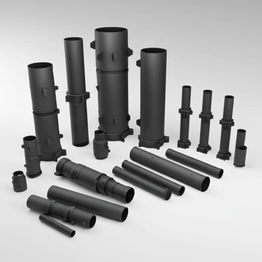
Types of SiC 3D Printing Technologies and Equipment
Several additive manufacturing technologies are being adapted and optimized for producing silicon carbide parts. Each method has its unique approach to building components layer by layer, and the choice of technology often depends on the desired part complexity, resolution, material properties, and production volume.
1. Binder Jetting
Binder Jetting is one of the more developed AM technologies for ceramics, including SiC.
- Process: A liquid binding agent is selectively deposited by an inkjet-style print head onto a thin layer of SiC powder. The build platform lowers, another layer of powder is spread, and the process repeats until the “green” part is formed.
- Post-Processing: The green part is fragile and requires careful de-powdering, followed by curing, debinding (to remove the binder), and sintering at high temperatures (often with infiltrants like molten silicon for Reaction Bonded Silicon Carbide – RBSC) to achieve densification and final properties.
- Advantages: Relatively fast build speeds, ability to create large parts, no need for support structures during printing (the powder bed supports overhangs).
- Considerations: Green parts have low strength; sintering and infiltration steps are crucial and can introduce shrinkage or dimensional changes. Porosity can be an issue if not properly processed.
2. Direct Ink Writing (DIW) / Robocasting
DIW involves extruding a highly concentrated SiC-based ink or paste through a fine nozzle.
- Process: A robotic system or gantry precisely dispenses the SiC ink layer by layer according to a CAD model. The ink is formulated to retain its shape after deposition.
- Post-Processing: Printed parts are dried and then sintered at high temperatures to densify the material.
- Advantages: Good control over material composition, potential for multi-material printing, ability to create complex internal structures and fine features.
- Considerations: Slower build speeds for large parts compared to binder jetting; careful formulation of the ink is critical for printability and final properties; support structures may be needed for complex overhangs.
3. Vat Photopolymerization (SLA/DLP with SiC-loaded Resins)
Stereolithography (SLA) or Digital Light Processing (DLP) can be adapted for SiC by using photocurable resins heavily loaded with SiC particles.
- Process: A light source (UV laser for SLA, projector for DLP) selectively cures the SiC-loaded resin layer by layer.
- Post-Processing: The “green” part, consisting of SiC particles held by a polymer binder, is cleaned of excess resin. It then undergoes a debinding process to remove the polymer, followed by sintering to fuse the SiC particles.
- Advantages: High resolution and fine feature detail, good surface finish.
- Considerations: Limited to the amount of SiC powder that can be loaded into the resin (typically affects final density and properties); debinding and sintering are critical and complex; shrinkage can be significant.
4. Material Considerations for SiC 3D Printing Equipment:
The choice of SiC powder is critical for successful 3D printing:
- Particle Size and Distribution: Affects powder bed density, flowability (for binder jetting), and sintering behavior. Finer particles generally aid sintering but can pose handling challenges.
- Morphology: Particle shape influences packing and flow. Spherical particles are often preferred.
- Purity: Impurities can affect the final properties of the SiC component, especially electrical and thermal characteristics.
- Additives/Binders: The type and amount of binders (in binder jetting and vat photopolymerization) or rheological agents (in DIW inks) must be carefully selected to ensure good printability and successful removal during post-processing.
The equipment itself typically includes precision motion systems, powder handling/spreading mechanisms (binder jetting), sophisticated print heads or extrusion systems, and controlled build environments. Post-processing often requires high-temperature furnaces capable of reaching sintering temperatures for SiC (often >2000°C) in controlled atmospheres.
Design Considerations for Manufacturing with SiC 3D Printers
Successfully manufacturing silicon carbide components using 3D printing requires more than just advanced equipment; it demands a thoughtful approach to design, often referred to as Design for Additive Manufacturing (DfAM). This involves optimizing the part’s geometry for the specific SiC 3D printing process being used, considering the material’s unique characteristics and the subsequent post-processing steps.
Key DfAM Principles for SiC:
- Wall Thickness:
- Minimum Wall Thickness: Each SiC 3D printing process has a minimum achievable wall thickness due to particle size, layer height, and green part strength. Designing below this can lead to print failures or damage during handling and post-processing.
- Maximum Wall Thickness: Very thick sections can be challenging for complete binder burnout during debinding and uniform sintering, potentially leading to internal defects or cracks. Consider incorporating internal voids or lattice structures for thicker parts.
- Feature Size and Resolution:
- Small features, holes, and channels must be designed within the resolution capabilities of the printer and SiC material system. Tiny, unsupported features may not form correctly or survive post-processing.
- Aspect ratios (height-to-width) of features should be considered to ensure stability.
- Overhangs and Support Structures:
- While binder jetting is self-supporting, other SiC AM processes like DIW or vat photopolymerization may require support structures for overhangs and bridges beyond a certain angle (typically >45 degrees).
- Supports should be designed for easy removal without damaging the part, especially given SiC’s hardness after sintering. Consider the material of the supports; sometimes sacrificial SiC supports are used.
- Designing self-supporting angles or tear-drop shaped holes can minimize the need for supports.
- Shrinkage and Distortion:
- SiC parts undergo significant shrinkage during sintering (can be 15-25% or more depending on the process and initial green density). This shrinkage must be accurately predicted and compensated for in the initial CAD design.
- Non-uniform shrinkage can lead to distortion or warping, especially in parts with varying cross-sections. Design for uniform wall thickness where possible or use simulation tools to predict and mitigate distortion.
- Internal Channels and Complex Geometries:
- One of the key strengths of AM is creating complex internal channels. Ensure channels are large enough for powder removal (binder jetting) or resin drainage (vat photopolymerization) and that they can withstand cleaning processes.
- Avoid sharp internal corners, which can be stress concentration points. Use fillets and radii.
- Part Orientation:
- The orientation of the part on the build plate can affect surface finish, accuracy, build time, and the amount of support needed. Anisotropic properties can also arise based on build direction.
- Orient parts to minimize supports on critical surfaces or to align layers for optimal strength in specific directions if applicable.
- Material Considerations during Design:
- If the part will be Reaction Bonded Silicon Carbide (RBSC), consider pathways for silicon infiltration.
- For Sintered Silicon Carbide (SSC), design to promote uniform densification.
- Tolerances:
- Understand the achievable tolerances of the chosen SiC AM process and post-processing steps. Design critical features with these tolerances in mind, and specify where secondary machining might be needed for tighter requirements.
Engaging with experienced SiC AM providers early in the design phase is crucial. They can offer guidance on material selection, process-specific DfAM rules, and predict potential manufacturing challenges, ultimately leading to a more successful and cost-effective outcome.
Post-Processing: Refining 3D Printed SiC Components
Creating a silicon carbide part via 3D printing is a multi-stage process, and the “as-printed” or “green” component is often far from its final functional state. Post-processing steps are critical to transform this green part into a dense, strong, and precise SiC component with the desired material properties and surface finish. The specific steps vary depending on the 3D printing technology used (e.g., binder jetting, DIW, vat photopolymerization).
1. De-powdering / Cleaning (Primarily for Binder Jetting & Powder-Bed Systems)
- Objective: To remove all loose, unbonded SiC powder from the green part, especially from internal channels and complex features.
- Methods: Gentle brushing, compressed air blowing, vacuuming. Care must be taken as green parts are fragile.
- Importance: Incomplete powder removal can lead to defects or unwanted fused material after sintering.
2. Curing / Pre-Sintering (If applicable)
- Objective: To strengthen the green part slightly for easier handling before the main debinding and sintering stages. This is often relevant for binder-jetted parts.
- Methods: Low-temperature oven heating to partially cure the binder.
3. Debinding (Binder Removal)
- Objective: To completely remove the organic binder (from binder jetting or photopolymer resins) from the green part, leaving behind a porous SiC structure (the “brown” part).
- Methods:
- Thermal Debinding: Slowly heating the part in a controlled atmosphere furnace to pyrolyze (burn out) the binder. The heating schedule must be very precise to avoid defects like cracking or bloating due to rapid gas evolution.
- Solvent Debinding: Sometimes used as a preliminary step to remove a portion of the binder before thermal debinding.
- Importance: Residual binder can contaminate the SiC during sintering and affect final properties. Incomplete debinding can cause defects.
4. Sintering / Infiltration
This is the most critical step for densification and achieving the final SiC material properties.
- Solid-State Sintering (for Sintered Silicon Carbide – SSC):
- Objective: To densify the porous brown part by heating it to very high temperatures (typically >2000°C, e.g., 2100-2300°C) in a controlled atmosphere (e.g., argon or vacuum). This causes the SiC particles to bond and fuse, reducing porosity. Sintering aids (like boron and carbon) are often used.
- Outcome: High-purity, dense SiC. Significant shrinkage occurs.
- Reaction Bonding / Infiltration (for Reaction Bonded Silicon Carbide – RBSC, also known as Siliconized Silicon Carbide – SiSiC):
- Objective: To densify the porous SiC preform by infiltrating it with molten silicon (typically around 1500-1700°C). The silicon reacts with free carbon (often added to the initial SiC powder mix or formed from binder pyrolysis) to form new, secondary SiC in-situ, which bonds the original SiC grains. Excess silicon fills remaining pores.
- Outcome: A dense composite of primary SiC, secondary SiC, and some free silicon (typically 8-15%). Less shrinkage compared to SSC. Often faster and less expensive than SSC.
- Liquid Phase Sintering (LPS-SiC): Uses sintering additives that form a liquid phase at high temperatures, aiding densification at slightly lower temperatures than SSC.
5. Surface Finishing & Machining
Even after sintering, the SiC part may require further processing to meet dimensional tolerances or surface finish requirements, especially since SiC is extremely hard.
- Grinding: Using diamond grinding wheels to achieve precise dimensions and flat surfaces.
- Lapping and Polishing: To achieve very smooth surfaces (e.g., for seals, bearings, or optical components). Diamond slurries are typically used.
- Laser Machining: Can be used for drilling small holes or creating fine features on sintered SiC.
- Electrical Discharge Machining (EDM): Applicable if the SiC grade has sufficient electrical conductivity (e.g., some RBSC grades with higher free silicon).
6. Cleaning and Inspection
- Objective: Final cleaning to remove any residues from machining or handling.
- Inspection: Dimensional checks, surface roughness measurement, NDT (Non-Destructive Testing) like X-ray or ultrasonic testing to detect internal flaws, and material characterization.
The complexity and precision required in these post-processing steps underscore the need for specialized equipment (high-temperature furnaces, diamond machining tools) and expertise. Achieving the desired tolerances (often in microns) and surface finishes (Ra values down to nanometers for polished surfaces) on a material as hard as SiC is a significant engineering challenge that adds to the overall manufacturing cost and lead time but is essential for high-performance applications.
Overcoming Challenges in SiC Additive Manufacturing
While Silicon Carbide (SiC) additive manufacturing (AM) offers transformative potential, its widespread adoption and industrialization come with a set of technical and economic challenges. Continuous research and development are focused on addressing these hurdles to make SiC 3D printing more robust, reliable, and cost-effective.
1. Material Consistency and Powder Quality:
- Challenge: The properties of the final SiC part are highly dependent on the characteristics of the starting powder (particle size, distribution, morphology, purity) and its interaction with binders or slurries. Ensuring lot-to-lot consistency of SiC powders specifically designed for AM is crucial.
- Mitigation:
- Development of standardized SiC powders optimized for different AM processes.
- Rigorous quality control of incoming raw materials.
- Improved powder spheroidization techniques for better flowability and packing density.
2. Achieving High Density and Desired Microstructure:
- Challenge: Attaining near-full theoretical density and controlling grain size are critical for optimal mechanical, thermal, and chemical properties. Porosity can be a significant issue, acting as stress concentrators and degrading performance. The debinding and sintering/infiltration stages are particularly sensitive.
- Mitigation:
- Optimizing printing parameters (layer thickness, binder saturation, laser power, etc.).
- Refining debinding schedules to prevent defects.
- Advanced sintering techniques (e.g., Spark Plasma Sintering (SPS) for R&D, optimizing pressure, temperature, and atmosphere in conventional sintering).
- Precise control over infiltration processes for RBSC to minimize residual porosity or unreacted silicon.
- Use of appropriate sintering aids for SSC.
3. Shrinkage Control and Dimensional Accuracy:
- Challenge: Significant and potentially non-uniform shrinkage occurs during sintering (especially for SSC), making it difficult to achieve tight dimensional tolerances without iterative design adjustments or post-machining.
- Mitigation:
- Accurate shrinkage prediction models and

About the Author: Sicarb Tech
We provide clear and reliable insights into silicon carbide materials, component manufacturing, application technologies, and global market trends. Our content reflects industry expertise, practical experience, and a commitment to helping readers understand the evolving SiC landscape.

Customizable SiC
You May Also Interest
-
![]()
Key SiC Exporters in Asia for International Trade
Key SiC Exporters in Asia for International Trade In the rapidly evolving landscape of advanced materials, silicon carbide (SiC) stands out as a material of unparalleled performance. Its exceptional properties make it indispensable across a spectrum of demanding industrial applications. For businesses seeking reliable and high-quality silicon carbide products, understanding the key players and regions…
-
![]()
SiC Substrates: Key to Electronic Device Advances
SiC Substrates: Key to Electronic Device Advances Introduction: The Pivotal Role of SiC Substrates In the rapidly evolving landscape of high-performance industrial applications, materials science plays a crucial role. Among advanced materials, silicon carbide (SiC) stands out, particularly in the form of SiC substrates. These substrates are not merely foundational layers; they are critical enablers…
-
![]()
SiC Innovation via University Research Links
SiC Innovation via University Research Links In the rapidly evolving landscape of advanced materials, custom silicon carbide (SiC) stands out as a true game-changer. Its unparalleled properties make it indispensable across a spectrum of demanding industrial applications, from the cutting edge of semiconductor manufacturing to the extreme environments of aerospace and nuclear energy. But what…