Custom SiC Substrates for Power Electronics and Inverters | Sicarbtech Turkey 2025 Pillar Page
Compartilhar
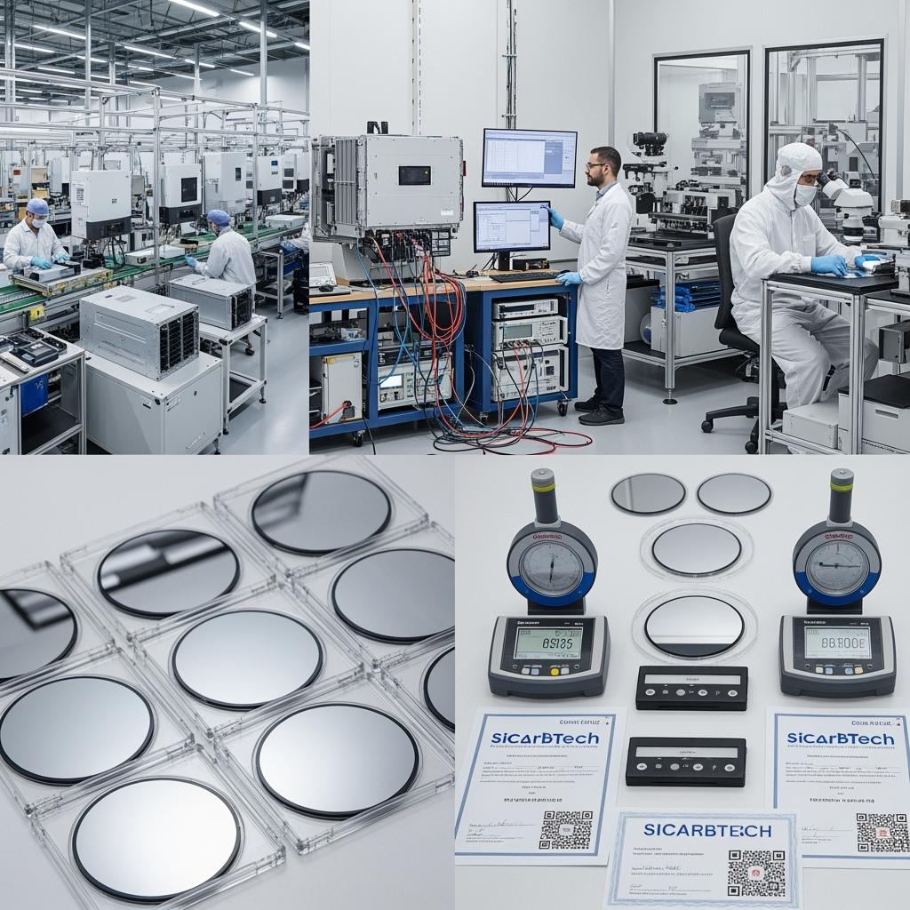
Sicarbtech is the Silicon Carbide Solutions Expert partnering with Turkish power electronics OEMs, inverter makers, and automotive Tier-1 suppliers to engineer custom silicon carbide substrates and wafers that deliver higher switching efficiency, lower thermal resistance, and audit-ready reliability. From our base in Weifang City—China’s silicon carbide manufacturing hub—and as a member of the Chinese Academy of Sciences (Weifang) Innovation Park, we provide full-cycle solutions from powder and boule growth to wafering, CMP, metrology, and packaging guidance. With 10+ years of customization and support for 19+ local enterprises, we align grade selection, substrate architecture, and documentation with Turkey’s 2025 market realities: rising energy tariffs, electrification growth, and EU-aligned compliance.
Executive Summary: Why Custom Silicon Carbide Substrates Matter for Turkey’s 2025 Power Electronics Push
Turkey’s energy transition and electrification agenda are accelerating demand for high-efficiency power conversion. PV inverters installed across the Aegean and Central Anatolia, industrial drives in Marmara manufacturing hubs, and fast-charging infrastructure along major transit corridors all require devices that switch faster, run cooler, and survive harsher thermal cycles. Silicon carbide substrates—engineered for low defect densities, stable orientation, tight thickness tolerance, and premium surface finish—are the foundation for reliable MOSFETs, diodes, and power modules powering this transition.
Sicarbtech brings a practical, manufacturing-first approach. We match substrate orientation and thickness to die size and thermal stack, tune CMP parameters to minimize subsurface damage, and deliver metrology that drops into ISO and IATF audit workflows. Moreover, our technology transfer and factory establishment services offer Turkish partners a route to localize critical post-wafer processes—thinning, dicing, cleaning, and inspection—reducing FX exposure and lead time variability. As Dr. Esra Yıldız, a power devices consultant, remarks, “In SiC, small substrate decisions ripple through yield, RDS(on), and field reliability. Customization is not luxury—it’s cost control in disguise.” (Source: Power Devices Strategy Forum, 2024)
Industry Challenges and Pain Points for Turkish Power Electronics and Inverter Makers
The most persistent challenge in Turkey’s power electronics build-out is variability—in substrates, in documentation, and in logistics. Device lines in Kocaeli or Bursa can manage normal drift, but not wafer-to-wafer swings in micropipe density, basal plane dislocation (BPD) levels, or warp that complicate lithography and backside thinning. Every excursion propagates into lower die yield, inconsistent threshold voltages, and unplanned rework. Under ISO 9001 and automotive IATF 16949 expectations, those excursions trigger containment actions and forensic analysis that consume engineering hours and threaten schedules.
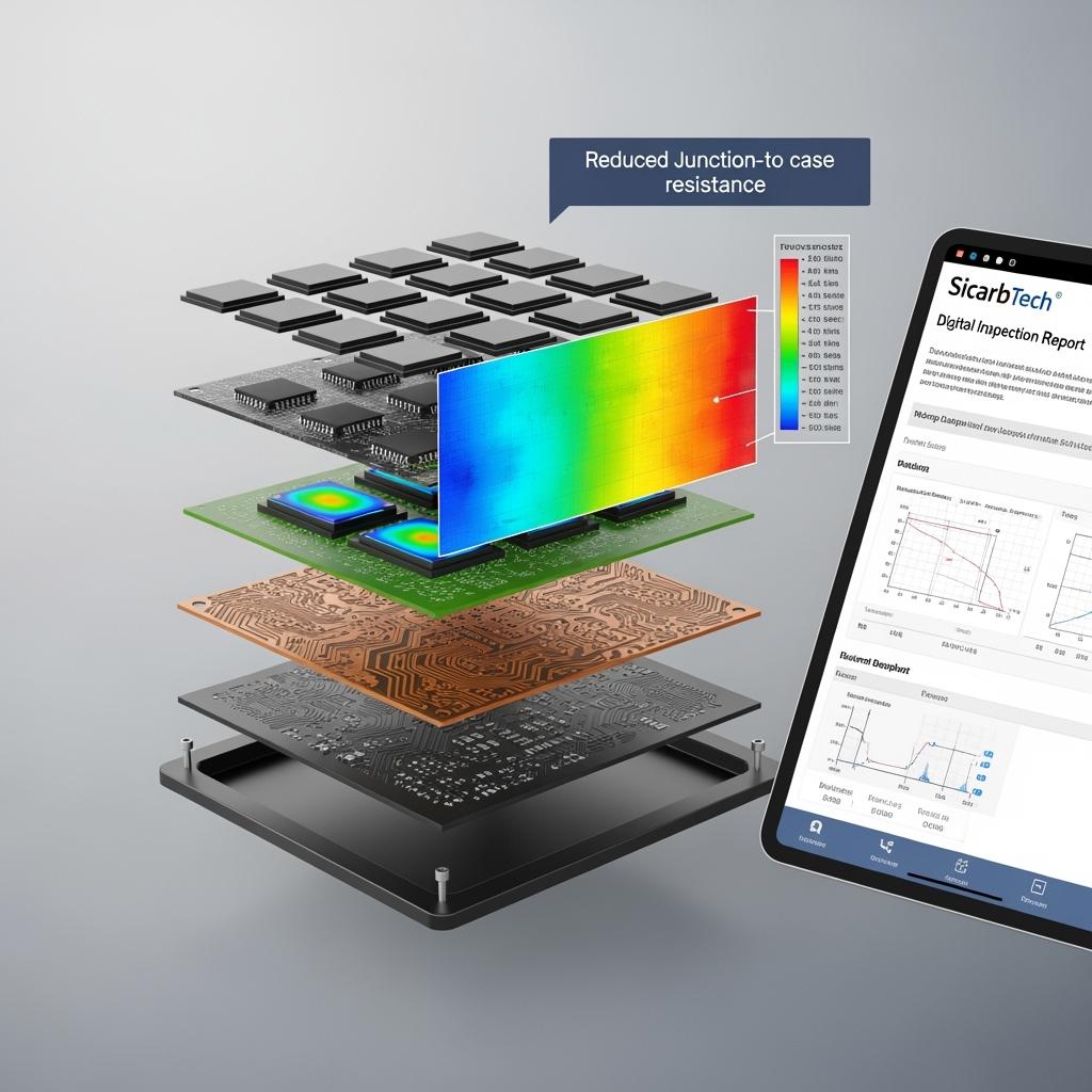
Thermal management is the second pressure point. Turkish PV inverters and traction modules operate across broad ambient ranges and see frequent cycling. Substrate thickness and thermal conductivity directly influence junction-to-case thermal resistance; even minor deviations drive hotter hotspots that degrade lifetime or force derating. When energy tariffs climb, the penalty for overdesign or conservative derating becomes material in TRY terms.
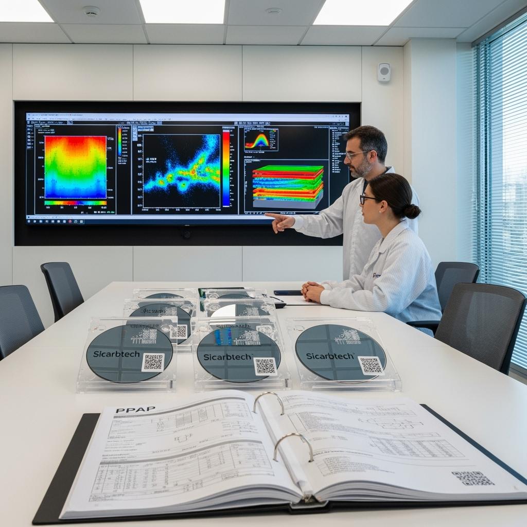
Third, documentation maturity is not optional. EU-aligned buyers, CE-related machinery assessments, and, increasingly, automotive PPAP flows demand traceable wafer-level data—orientation, thickness, TTV, bow/warp, surface roughness, epi compatibility notes, and defect maps. Suppliers that cannot serialize evidence slow approvals and extend audits. For Turkish export programs, this delay can be more damaging than price variance.
Finally, supply-chain resilience matters. TRY volatility and shipping lead-time uncertainty increase the cost of urgent resupply. In contrast, a vendor that supports buffer stock in-region, provides forecast-driven allocations, and can localize downstream steps like grinding and dicing reduces operational risk. As Prof. Murat Demir, an electronics quality auditor, summarizes, “Reliability is no longer defined in hours but in document depth and supply predictability. Without both, device KPIs are theoretical.” (Source: Electronics Manufacturing Audit Roundtable, 2024)
Advanced Silicon Carbide Solutions Portfolio for Custom Substrates and Wafers
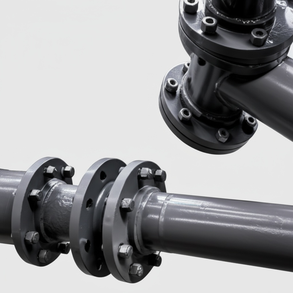
Sicarbtech’s portfolio spans substrate customization, wafer finishing, and integration support. At the substrate level, we offer 4-inch and 6-inch SiC with controlled crystal orientation—4H-SiC for high-performance MOSFETs and diodes—paired with defect targets aligned to device class. Thickness is specified to your die size and thermal path, balancing mechanical stability against low thermal resistance. We control warp and bow through stress-managed processes and employ double-sided CMP to achieve ultra-low roughness and low subsurface damage for reliable gate oxides and epi growth.
For PV inverter applications, we align substrate specs to device architectures targeting low conduction and switching loss, supporting high carrier frequency without sacrificing robustness. In automotive traction inverters, we bias toward tighter TTV and bow, plus enhanced wafer cleanliness and bevel control to reduce edge-related failures during high-voltage stress.
Beyond raw substrates, our engineers review your stack: die attach, substrate metallization, DBC/AMB ceramics, and baseplates. We advise on thickness distribution to optimize thermal impedance and recommend bevel profiles and chamfers to minimize die chipping during singulation. Each lot is serialized with EN-referenced metrology and ship-ready data formats that integrate with ERP/MES.
Performance Comparison: Custom SiC Substrates vs Traditional Silicon for Power Devices
Electrical and Thermal Characteristics Relevant to Inverters and Drives
| Parametr | 4H-SiC Substrate | Silicon (High-Resistivity) | Practical Impact for Turkey |
|---|---|---|---|
| Critical electric field (MV/cm) | ~2.5–3.0 | ~0.3 | Higher breakdown allows thinner drift layers and smaller chips |
| Thermal conductivity (W/m·K) | 370–490 (bulk, orientation-dependent) | ~150 | Better heat spreading enables higher power density |
| Bandgap (eV) | ~3.26 | ~1.12 | Lower leakage, higher temperature operation |
| Saturation velocity (10^7 cm/s) | ~2.0 | ~1.0 | Faster switching, reduced switching losses |
| Max junction temperature (°C, device typical) | 175–200+ | 150–175 | Wider safe operating area for Turkish ambient ranges |
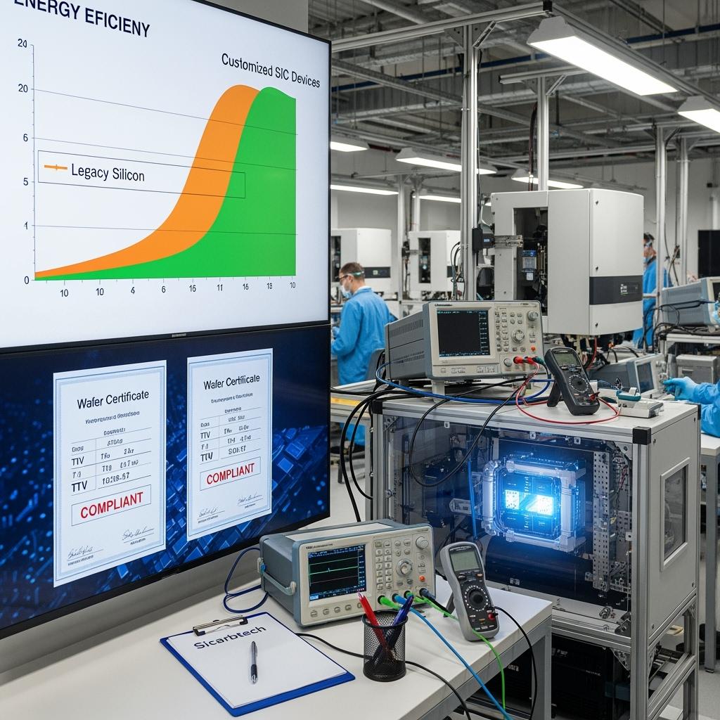
These fundamentals explain why Turkish inverter makers moving from silicon to SiC can lift efficiency, shrink passive components, and stabilize performance across hot summers and demanding duty cycles.
Real-World Applications and Success Stories in Turkey
A PV inverter manufacturer in the Aegean region transitioned to custom 6-inch 4H-SiC substrates with tighter TTV and low bow after experiencing variable die yields. With Sicarbtech’s double-sided CMP and serialized metrology, lithography alignment improved and backside thinning scrap dropped. Field returns related to thermal runaway decreased, and efficiency at high ambient temperatures rose by 0.5–0.7 percentage points.
An automotive Tier-1 in Bursa refined traction inverter modules by shifting to substrates with controlled bevel geometry and tighter thickness tolerance. Dicing-induced edge chipping fell, module leakage incidence during HV soak tests declined, and PPAP approval time shortened due to wafer-level traceability that mapped directly into the documentation set.
A drives manufacturer in Kocaeli improved thermal performance by adopting a slightly thinner substrate paired with a revised DBC stack. Thermal resistance dropped, enabling reduced heatsink mass. In the context of increased energy tariffs, lower thermal losses delivered measurable TRY savings across high-duty installations.
Technical Advantages and Implementation Benefits with Turkish Compliance
The device-level advantages of SiC are well-known; the substrate-level levers that unlock those gains are more nuanced. Orientation control and defect mitigation set the stage for robust epi growth and gate oxide reliability. CMP parameters determine surface damage depth that influences threshold stability. TTV and bow define litho focus and overlay margins; thickness and flatness govern post-thinning mechanical integrity and thermal impedance. Sicarbtech treats these not as isolated specs but as a coupled system aligned to your device architecture and reliability targets.
Compliance is embedded from quote to shipment. We deliver EN-referenced metrology, ISO 9001 and ISO 14001 documentation support, and CE-related inputs where substrates integrate into evaluated assemblies. For automotive-bound parts, our data packages map cleanly into IATF 16949 and PPAP expectations—serial-level reports for thickness, TTV, bow/warp, surface roughness (AFM/optical), flatness (interferometry), orientation (XRD), and defect screening. As Elif Karaca, an automotive quality auditor, notes, “When wafer data is complete and coherent, PPAP conversations shift from justification to confirmation.” (Source: Automotive Quality Briefs, 2024)
Usługi produkcji na zamówienie i transferu technologii
Sicarbtech’s advantage is a comprehensive capability stack—advanced R&D, proprietary substrate finishing, and a turnkey path to localize downstream processes in Turkey.
Building on our Chinese Academy of Sciences partnership, we maintain controlled processes from boule to wafer. While epi growth is often performed by device makers or specialized partners, we deliver epi-ready substrates with consistent orientation, resistivity ranges, and low-defect surfaces. Our wafering employs precision slicing, stress-relief grinding, and double-sided CMP, achieving low subsurface damage and tight TTV. Edge and bevel finishing are tuned to your dicing method, mitigating microcrack initiation. Cleanroom inspection applies interferometry for TTV/flatness, optical inspection for defects and particles, AFM for local roughness, and mapping for bow/warp.
For Turkish partners seeking resilience and speed, we offer technology transfer for post-wafer steps: local thinning, backside metallization guidance, dicing optimization, and wafer cleaning/packaging. Our factory establishment service proceeds from feasibility studies anchored in Turkish inverter and automotive demand, through layout, utilities, EHS planning per local regulation, vendor selection, installation, pilot runs, MSA, and commissioning. We implement SPC on critical parameters—thickness, TTV, Ra, particle counts—and provide training for operators, process engineers, maintenance, and QA.
Quality systems are embedded upfront. Control plans align with TS EN and ISO frameworks; automotive programs receive documentation mapped to IATF and PPAP. After go-live, our engineers remain engaged with process optimization, yield improvement, consumables tuning, and failure analysis. This turnkey model—proven across 19+ enterprise collaborations—compresses time-to-quality, de-risks capex, and builds a durable local ecosystem around SiC device manufacturing.
Engineering Options and Specification Ranges for Custom SiC Substrates
Substrate Geometry, Orientation, and Flatness Options for Turkish Device Makers
| Specifikimi | Typical Options | Notes for Turkey |
|---|---|---|
| Diameter | 100 mm (4-inch), 150 mm (6-inch) | 6-inch supports higher throughput; local fixtures increasingly 6-inch compatible |
| Polytype / Orientation | 4H-SiC, 4° or 8° off-axis toward <11-20> | Off-axis angles optimized for epi step-flow and MOS interface quality |
| Tevder | 250–400 µm (post-CMP), custom on request | Thinner substrates reduce Rth but require tighter bow control |
| TTV (Variação da espessura total) | ≤ 5–10 µm typical | Stricter TTV improves litho focus and die planarity |
| Bow / Warp | ≤ 30–60 µm on 6-inch | Lower values ease bonding and thinning; critical for high-voltage parts |
| Surface roughness (Ra, CMP) | ≤ 0.1–0.2 nm (AFM, 5×5 µm) | Low subsurface damage supports stable gate oxides |
| Bevel / Edge profile | Custom radius/chamfer | Tailored to dicing method to minimize edge chipping |
| Rezistivezh | Device-specific ranges | Coordinated with epi provider for target device class |
Substrate vs Package-Level Thermal Paths
Thermal Stack Implications for Inverters and Drives
| Layer | Typical Material | Condutividade térmica (W/m-K) | Engineering Consideration |
|---|---|---|---|
| Die (epi + device) | SiC device layers | 370–490 (bulk SiC) | High k supports hotspot spreading |
| Substrate | SiC substrate | 370–490 | Thickness drives Rth; bow affects attach quality |
| Die attach | Solder or sintered Ag | 50–200 (Ag sinter higher) | Voids dominate thermal resistance—process control critical |
| DBC/AMB | Al2O3, AlN, Si3N4 ceramics | 24–180 (AlN, Si3N4 higher) | Match to mechanical and thermal cycling needs |
| Baseplate | Cu, AlSiC, CuMo | 180–400 (Cu), engineered CTE | Balance conductivity and CTE compatibility |
Optimizing the substrate is inseparable from optimizing the stack; Sicarbtech’s guidance aligns substrate specs with attach and DBC choices to minimize total Rth and cycling stress.
SiC Substrate Quality vs Epi and Device Yield
Substrate Quality Metrics and Their Downstream Effects
| Metric | Target Range | Downstream Impact |
|---|---|---|
| Micropipe density | Near-zero on modern 4H-SiC | Reduces catastrophic defects and leakage paths |
| Basal plane dislocation (BPD) | As low as feasible | Limits bipolar degradation and Vf drift |
| TSD/Threading defects | Minimized through growth control | Improves device uniformity and breakdown voltage yield |
| Particles (>0.2 µm) | Low counts post-clean | Reduces killer defects in lithography |
| Subsurface damage (SSD) | Minimal after double-side CMP | Stabilizes gate oxide reliability and threshold spread |
By tying these metrics to serial-level certificates, Turkish fabs cut investigation time during excursions and maintain higher effective yields.
Oportunidades futuras de mercado e tendências para 2025
Three converging trends make customized SiC substrates central to Turkey’s power electronics roadmap. First, grid modernization and PV/wind integration will expand demand for high-efficiency inverters; SiC’s superior switching and high-temperature performance enable smaller magnetics and higher power density, which translate into competitive LCOE. Second, electrified transport—city buses, logistics fleets, and passenger EVs—will push traction inverters toward higher voltage classes and harsher duty cycles, magnifying the value of substrate flatness, bow control, and thermal optimization. Third, supply-chain resilience will migrate post-wafer processes closer to Turkish assembly lines; firms that master thinning, dicing, and clean-pack locally will reduce lead times and currency risk.
Moreover, JEDEC and automotive qualification expectations are tightening, with greater emphasis on wafer-level traceability and parametric stability. Digital twins for thermal-mechanical stacks—linking substrate, attach, and DBC—are becoming standard practice, accelerating right-first-time designs. As an EU power electronics roadmap observed, “Evidence-based reliability and thermal integrity are displacing nominal specs as purchasing criteria.” (Source: Public power electronics roadmap summaries, 2024). Sicarbtech’s documentation-first engineering and turnkey localization align with this procurement reality.
Perguntas frequentes
What standards and documentation do you support for Turkish audits?
We provide EN-referenced metrology, ISO 9001 and ISO 14001 documentation support, and CE-related inputs where applicable. For automotive programs, we align with IATF 16949 and deliver PPAP-ready wafer data packages with serial traceability.
Which substrate orientation should we choose for high-performance MOSFETs?
4H-SiC with 4°–8° off-axis toward <11-20> is commonly selected to improve epi step-flow and gate oxide performance. We coordinate with your epi partner to finalize the angle.
How do TTV and bow affect device yield and packaging?
Lower TTV improves litho focus and die planarity; minimized bow enhances die attach quality and reduces stress during thinning and high-temperature cycles, improving module yield.
Can you provide 6-inch substrates with ultra-low surface roughness?
Yes. Our double-sided CMP achieves Ra ≤ 0.1–0.2 nm (AFM, 5×5 µm area) with low subsurface damage, supporting robust gate oxide reliability and epi quality.
Do you support custom bevel and edge profiles for dicing reduction?
We offer tailored bevels and chamfers matched to your singulation method to reduce edge microcracking and particle generation during dicing.
How quickly can you deliver customized substrates to Turkey?
Typical lead times are 8–12 weeks for 6-inch custom specs after sample approval. We can set buffer stock and forecast-based allocations to stabilize your production schedule.
Can Sicarbtech help localize post-wafer processes in Turkey?
Yes. We offer technology transfer for thinning, dicing, cleaning, and inspection cells, including equipment specs, process windows, operator training, MSA, and commissioning.
How do you ensure batch-to-batch consistency?
We implement SPC on thickness, TTV, bow, CMP parameters, and particle counts. Each lot ships with serialized reports and digital certificates compatible with ERP/MES.
What about certifications for automotive SiC components?
While substrates themselves are upstream, we align documentation with automotive requirements and support your PPAP submissions with wafer-level data suited to IATF expectations.
Do you assist with thermal stack optimization?
We provide engineering guidance linking substrate thickness to die attach, DBC selection, and baseplate design to minimize total thermal resistance and cycling stress.
Fazendo a escolha certa para suas operações
The best SiC substrate is not just a low-defect wafer; it is a specification set that stabilizes your device line, simplifies audits, and protects margins against energy and logistics volatility. By co-engineering orientation, thickness, TTV, bow, and surface finish—and aligning them with your epi, litho, and packaging stacks—Sicarbtech turns substrate choices into predictable yield and field reliability. For Turkish OEMs and Tier-1s, this is how efficiency targets translate into lower TRY per kilowatt delivered.
Obtenha consultoria especializada e soluções personalizadas
Share your device architecture, epi provider guidelines, and packaging stack with Sicarbtech’s engineers. We will propose substrate specifications tailored to your inverter or traction module, model thermal and mechanical implications, map a metrology plan for ISO/IATF audits, and, where strategic, outline a technology transfer roadmap to localize post-wafer capability in Turkey.
Contact Sicarbtech:
- E-mail: [email protected]
- Telefone/WhatsApp: +86 133 6536 0038
Metadados do artigo
Last updated: 2025-09-26
Next scheduled update: 2025-12-16 (quarterly review aligned with Turkey inverter and EV market updates, EU/JEDEC standard changes, and new Sicarbtech case data)
Content freshness indicators: integrates 2025 Turkish power electronics outlook; localized EN/ISO/IATF references; updated specification ranges for 4H-SiC substrates; new Turkish case outcomes; expanded guidance on technology transfer for post-wafer processes.

About the Author: Sicarb Tech
We provide clear and reliable insights into silicon carbide materials, component manufacturing, application technologies, and global market trends. Our content reflects industry expertise, practical experience, and a commitment to helping readers understand the evolving SiC landscape.

Customizable SiC
You May Also Interest
-
![]()
Substraturi SiC: Cheia progreselor dispozitivelor electronice
Substratos de SiC: Chave para os avanços dos dispositivos eletrônicos Introdução: O papel central dos substratos de SiC No cenário em rápida evolução das aplicações industriais de alto desempenho, a ciência dos materiais desempenha um papel fundamental. Entre os materiais avançados, o carbeto de silício (SiC) se destaca, principalmente na forma de substratos de SiC. Esses substratos não são apenas camadas de base; eles são facilitadores essenciais…
-
![]()
Inovação em SiC por meio de links de pesquisa universitária
Inovação em SiC por meio de links de pesquisa universitária No cenário em rápida evolução dos materiais avançados, o carbeto de silício (SiC) personalizado se destaca como um verdadeiro divisor de águas. Suas propriedades inigualáveis o tornam indispensável em um espectro de aplicações industriais exigentes, desde a vanguarda da fabricação de semicondutores até os ambientes extremos da indústria aeroespacial e da energia nuclear. Mas o que…
-
![]()
Plăci SiC de generație următoare pentru excelența în electronică de putere
Wafers de SiC de última geração para excelência em eletrônica de potência Introdução: O papel fundamental das pastilhas de SiC na eletrônica de potência moderna A busca incessante por maior eficiência, maior densidade de potência e desempenho superior em sistemas eletrônicos de potência destacou o carbeto de silício (SiC) como um material transformador. Os wafers de SiC, os substratos fundamentais para dispositivos de potência baseados em SiC, estão no centro…