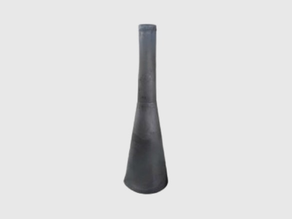
Precision SiC Laser Processing for Intricate Designs
Share
Precision SiC Laser Processing for Intricate Designs
Introduction: The Cutting Edge of Silicon Carbide Machining
Silicon Carbide (SiC) stands as a cornerstone material in high-performance industrial applications due to its exceptional properties, including superior hardness, high thermal conductivity, excellent wear resistance, and chemical inertness. However, these very characteristics make SiC notoriously difficult to machine using traditional methods. As industries demand increasingly complex and miniaturized components, precision SiC laser processing has emerged as a transformative technology. This advanced manufacturing technique enables the creation of intricate designs and fine features in SiC parts that were previously unachievable, opening new frontiers for innovation in sectors like semiconductors, aerospace, and power electronics. Laser processing offers a non-contact method, minimizing mechanical stress and tool wear, making it ideal for this ultra-hard ceramic material. This blog post delves into the nuances of SiC laser processing, its applications, advantages, and crucial considerations for businesses looking to leverage this cutting-edge technology for their custom silicon carbide components.
Why Laser Processing for Silicon Carbide’s Intricate Designs?
Traditional machining methods for silicon carbide, such as grinding and lapping, often struggle with producing complex geometries, fine details, and sharp features. They can also induce micro-cracks and subsurface damage, compromising the integrity of the SiC component. Laser processing of SiC overcomes these limitations by offering several distinct advantages:
- Non-Contact Machining: Lasers ablate or vaporize material without physical contact, eliminating tool wear and reducing mechanical stress on the workpiece. This is critical for brittle materials like SiC.
- High Precision and Accuracy: Focused laser beams can achieve micron-level precision, enabling the creation of extremely fine features, holes, channels, and complex 2D/3D patterns.
- Minimal Heat Affected Zone (HAZ): Advanced laser systems, particularly ultrashort pulse lasers (femtosecond and picosecond), minimize the heat affected zone. This “cold ablation” process reduces thermal damage, micro-cracking, and changes in material properties around the processed area.
- Design Flexibility: Laser systems are digitally controlled, allowing for rapid prototyping and easy modification of designs. Complex paths and intricate patterns can be programmed directly from CAD models.
- Versatility: Laser processing can perform various operations, including cutting, drilling, scribing, grooving, etching, and surface texturing on SiC substrates and components.
- Reduced Post-Processing: Due to the precision and quality of laser-machined surfaces, subsequent finishing steps can often be minimized or eliminated, saving time and cost.
For manufacturers requiring custom SiC components with sophisticated designs, laser processing offers unparalleled capabilities, pushing the boundaries of what’s possible with this advanced ceramic.
Key Industrial Applications of SiC Laser Processing
The unique capabilities of SiC laser processing make it indispensable across a wide array of demanding industries. Here’s a look at some prominent applications:
| Industry | Specific Applications of SiC Laser Processing | Benefits |
|---|---|---|
| Semiconductors | Dicing of SiC wafers, manufacturing of wafer chucks, etching of micro-channels for cooling, fabrication of components for MOCVD/CVD reactors (e.g., showerheads, injector nozzles). | High precision, reduced chipping, improved yield, ability to create complex micro-features for enhanced device performance. |
| Power Electronics | Structuring of SiC substrates for MOSFETs and diodes, isolation scribing, manufacturing of heat sinks and spreaders with intricate cooling channels. | Enhanced thermal management, improved device reliability, higher power density. |
| Aerospace & Defense | Fabrication of lightweight, high-stiffness mirrors and optical benches, components for rocket nozzles, thrusters, and hypersonic vehicle leading edges, sensor components. | High strength-to-weight ratio, thermal stability, wear resistance in extreme environments. |
| LED Manufacturing | Scribing and dicing of SiC substrates for LEDs, patterning for improved light extraction. | Increased manufacturing efficiency, higher brightness LEDs. |
| Automotive | Components for electric vehicle (EV) power modules, parts for braking systems, wear-resistant seals and bearings. Laser texturing for improved tribological properties. | Enhanced performance and durability, support for high-voltage EV systems. |
| Medical Devices | Manufacturing of precision surgical tools, biocompatible implants, components for diagnostic equipment requiring high wear resistance and stability. | Biocompatibility, sterilizability, precision for critical medical applications. |
| Chemical Processing | Fabrication of corrosion-resistant pump components, valves, seals, and nozzles for handling aggressive chemicals at high temperatures. | Excellent chemical inertness, long service life in harsh environments. |
| Industrial Machinery | Production of wear-resistant parts like bearings, mechanical seals, nozzles for abrasive fluid handling, and components for high-temperature furnaces. | Extended component lifetime, reduced maintenance, improved operational efficiency. |
The versatility of laser processing ensures that as new applications for SiC emerge, this technology will be at the forefront of enabling their realization, particularly for technical ceramic components requiring fine details.
Advantages of Precision SiC Laser Processing for Your Components
Choosing precision laser processing for your silicon carbide components unlocks a host of advantages that translate into superior product performance and manufacturing efficiency. These benefits are particularly crucial for B2B buyers, OEMs, and technical procurement professionals seeking high-quality, reliable SiC parts.
- Unmatched Geometric Complexity: Laser processing allows for the creation of highly complex 2D and 3D geometries, including internal cavities, undercuts (with specific laser techniques), and intricate surface patterns that are impossible or prohibitively expensive with conventional machining.
- Superior Accuracy and Repeatability: Modern laser systems offer exceptional positional accuracy and repeatability, ensuring that every component meets stringent dimensional specifications. This is vital for applications in semiconductors and aerospace where tolerances are tight.
- Minimal Thermal Damage: The use of ultrashort pulse lasers (femtosecond or picosecond) results in “cold ablation,” where material is removed with minimal heat transfer to the surrounding area. This significantly reduces the Heat Affected Zone (HAZ), preventing micro-cracks, phase changes, or degradation of SiC’s desirable properties.
- Enhanced Surface Quality: Laser processing can produce smooth surface finishes on SiC, often reducing the need for extensive post-processing steps like grinding or lapping. Specific laser parameters can also be tuned to achieve desired surface textures for applications like improved adhesion or tribology.
- No Tool Wear: Being a non-contact process, laser machining eliminates the costs and downtime associated with tool wear and replacement, which is a significant issue when machining ultra-hard SiC with conventional tools.
- Material Versatility within SiC Grades: Laser processing can be adapted for various types of silicon carbide, including sintered SiC (SSiC), reaction-bonded SiC (RBSiC), and chemical vapor deposited (CVD) SiC, by adjusting laser parameters.
- Rapid Prototyping and Production: The digital nature of laser processing allows for quick design changes and rapid iteration, making it ideal for prototyping. Once parameters are optimized, it can also be scaled for efficient series production of custom silicon carbide products.
- Cost-Effectiveness for Complex Parts: While the initial investment in laser processing equipment can be high, for complex parts or those requiring high precision, it can be more cost-effective in the long run due to reduced material waste, lower labor costs, and elimination of tooling expenses.
By leveraging these advantages, companies can gain a competitive edge, producing innovative SiC components with superior performance and reliability.
Types of Lasers Utilized for Silicon Carbide Processing
The choice of laser is critical for achieving optimal results in SiC processing. Different laser types offer varying characteristics in terms of wavelength, pulse duration, and power, making them suitable for specific applications and SiC grades.
- Ultrashort Pulse Lasers (Femtosecond and Picosecond):
- Femtosecond Lasers (pulse duration ~10-15 s): These are often considered the gold standard for high-precision SiC machining. The extremely short pulse duration leads to “cold ablation,” where material is vaporized almost instantaneously with minimal thermal energy transferred to the bulk material. This results in negligible HAZ, no recast layer, and exceptionally clean cuts and features. Ideal for micro-machining, drilling fine holes, and creating intricate patterns with the highest quality.
- Picosecond Lasers (pulse duration ~10-12 s): Offering a balance between femtosecond lasers and longer pulse lasers, picosecond lasers also provide excellent processing quality with minimal thermal damage. They can achieve higher ablation rates than femtosecond lasers for certain applications, making them suitable for tasks like scribing, grooving, and high-speed patterning.
- Nanosecond Lasers (e.g., UV, Green, IR):
- UV Lasers (e.g., Excimer, frequency-tripled Nd:YAG): Silicon carbide has strong absorption in the ultraviolet spectrum. UV lasers, with their shorter wavelengths (e.g., 355 nm, 266 nm), allow for better energy absorption at the surface, leading to more efficient material removal and finer features compared to IR lasers. They are widely used for scribing, dicing, and drilling SiC. The HAZ is more significant than with ultrashort pulse lasers but can be managed.
- Green Lasers (e.g., frequency-doubled Nd:YAG): With wavelengths around 532 nm, green lasers offer a compromise between UV and IR lasers in terms of absorption and cost. They are effective for various SiC machining tasks, including cutting and drilling thicker sections where higher power is beneficial.
- Infrared (IR) Lasers (e.g., Nd:YAG, Fiber Lasers): While SiC is somewhat transparent to IR wavelengths at room temperature, high-power IR lasers can still process SiC, particularly through multi-photon absorption or by initiating plasma. They are often used for rough cutting or deep drilling where speed is prioritized over the finest surface quality. The HAZ is typically larger with IR lasers.
The selection process involves considering the specific SiC material grade (e.g., reaction-bonded SiC vs. sintered SiC), the desired feature size and quality, processing speed requirements, and overall cost-effectiveness. For intricate designs requiring minimal thermal impact, ultrashort pulse lasers are generally preferred.
Achievable Precision and Designing for Intricate Features in SiC
Laser processing has revolutionized the ability to create highly precise and intricate features in silicon carbide components. Understanding the achievable limits and design considerations is crucial for engineers and designers.
Achievable Precision:
- Feature Sizes: With ultrashort pulse lasers, feature sizes can be in the range of a few micrometers (µm) to tens of micrometers. This includes hole diameters, channel widths, and kerf widths for cutting.
- Tolerances: Dimensional tolerances can typically be held within ±5 µm to ±25 µm, depending on the complexity of the feature, the thickness of the material, and the laser system used. Tighter tolerances often require more sophisticated process control and potentially slower processing speeds.
- Edge Quality: Laser processing, especially with femtosecond or picosecond lasers, can produce sharp, clean edges with minimal chipping or burring. This is a significant advantage over mechanical methods.
- Surface Roughness (Ra): Depending on the laser parameters and SiC grade, laser-machined surfaces can achieve Ra values from sub-micron levels up to a few microns. Post-processing (like fine polishing) may still be needed for applications requiring extremely smooth surfaces (e.g., optical mirrors).
Design Considerations for Intricate Features:
- Aspect Ratio: When drilling holes or cutting deep channels, the aspect ratio (depth-to-width ratio) is a critical parameter. Lasers can achieve high aspect ratios, but there are limits depending on the laser type and focusing optics. Deep, narrow features may require specialized techniques to manage debris removal and maintain beam quality.
- Material Thickness: The thickness of the SiC workpiece influences the choice of laser and processing speed. Thicker materials may require multiple passes or higher laser power, potentially affecting precision and HAZ.
- Minimum Wall Thickness: When designing closely spaced features or thin walls, ensure the design accounts for the material’s inherent brittleness and potential thermal stresses, even with “cold ablation.” Consult with your laser processing provider for guidelines.
- Corner Radii: Lasers naturally produce small corner radii due to the beam diameter. Achieving perfectly sharp internal corners can be challenging. Specify acceptable corner radii in your design.
- Taper Angle: Laser-cut or drilled features may exhibit a slight taper, especially in thicker materials. This can be minimized with optimized process parameters and beam shaping techniques. If taper is critical, it should be specified.
- CAD File Preparation: Provide clean, accurate CAD files (e.g., DXF, DWG, STEP) with clearly defined features and tolerances. This ensures smooth translation to the laser control software.
- Material Grade: Different SiC grades (e.g., porous, dense, CVD) absorb laser energy differently and have varying thermal and mechanical properties. The design should be compatible with the chosen SiC grade, and the laser process must be tuned accordingly. For instance, CVD SiC might allow for finer features due to its high purity and density.
Collaborating closely with an experienced SiC laser processing specialist during the design phase can help optimize for manufacturability, ensuring that intricate designs are realized with the desired precision and quality.
Material Considerations: Suitable SiC Grades for Laser Processing
While laser processing is versatile, the specific grade of silicon carbide significantly influences the machining process and outcomes. Understanding these nuances is key for procurement managers and engineers selecting materials for their applications.
| SiC Grade | Characteristics | Laser Processability & Considerations |
|---|---|---|
| Sintered Silicon Carbide (SSiC) / Direct Sintered SiC (DSSiC) | High density (>98%), fine grain size, excellent strength, hardness, and corrosion resistance. Pure SiC. | Generally processes well with ultrashort pulse lasers (femtosecond, picosecond) for high precision and minimal HAZ. UV and green nanosecond lasers can also be effective. Its homogeneity allows for consistent ablation. Ideal for demanding applications requiring high-purity SiC components. |
| Reaction-Bonded Silicon Carbide (RBSiC) / Silicon Infiltrated SiC (SiSiC) | Composite material containing SiC grains and free silicon (typically 8-20%). Good thermal conductivity, moderate strength, excellent wear resistance. | The presence of free silicon can affect laser interaction. Silicon has a lower melting/vaporization point than SiC. This can sometimes lead to preferential removal of silicon or different ablation characteristics compared to pure SiC. Ultrashort pulse lasers are preferred to minimize differential effects and HAZ. Careful parameter optimization is crucial. Often a cost-effective choice for industrial SiC components. |
| Nitride-Bonded Silicon Carbide (NBSiC) | SiC grains bonded by a silicon nitride phase. Good thermal shock resistance, moderate strength. Often porous. | Porosity can influence laser absorption and surface finish. Laser processing can be used, but edge quality and internal surface roughness might be affected by the porous structure. Parameter tuning is important to avoid excessive melting of the binder phase or internal cracking. |
| Chemical Vapor Deposited Silicon Carbide (CVD SiC) | Ultra-high purity (99.999%+), fully dense, excellent chemical resistance and thermal stability. Often used as coatings or for producing high-purity components. | Excellent for laser processing due to its purity and homogeneity. Allows for extremely fine features and smooth surfaces. Ultrashort pulse lasers are ideal for maintaining its pristine quality during micromachining. Used for semiconductor grade SiC applications. |
| Recrystallized Silicon Carbide (RSiC) | Typically porous, formed by firing compacted SiC grains at high temperatures. Excellent thermal shock resistance. | Similar to NBSiC, porosity is a key factor. Laser processing can be challenging for achieving very fine, sharp features due to the grain structure and porosity. Often used for kiln furniture and furnace components. |
| Graphite Loaded or Modified SiC | SiC with graphite additions to enhance specific properties like thermal conductivity or machinability (though still hard). | The presence of graphite can aid in laser absorption, potentially making it easier to process with a wider range of lasers. However, the differing ablation rates of SiC and graphite need to be managed for uniform results. |
Key considerations when selecting an SiC grade for laser processing include:
- Purity Requirements: Applications in the semiconductor industry often demand high-purity grades like SSiC or CVD SiC.
- Thermal Properties: The material’s thermal conductivity and coefficient of thermal expansion will affect how it responds to laser energy.
- Mechanical Properties: Hardness and fracture toughness influence material removal rates and potential for micro-cracking.
- Porosity: Porous materials may have different absorption characteristics and can result in rougher machined surfaces.
- Desired Feature Resolution: Denser, finer-grained materials like SSiC or CVD SiC generally allow for higher precision and finer features.
It is always recommended to discuss your specific application and material choice with a technical ceramics expert specializing in laser processing to ensure optimal results.
Common Challenges in SiC Laser Processing and Mitigation Strategies
Despite its numerous advantages, laser processing of silicon carbide is not without its challenges. Understanding these potential issues and how to mitigate them is crucial for successful implementation.
- Micro-cracking and Brittleness:
- Challenge: SiC is inherently brittle. Even with precise laser control, thermal stresses (though minimized with ultrashort pulses) can sometimes induce micro-cracks, especially with longer pulse lasers or aggressive processing parameters.
- Mitigation:
- Employ ultrashort pulse lasers (femtosecond/picosecond) to achieve “cold ablation” and minimize the Heat Affected Zone (HAZ).
- Optimize laser parameters: fluence, pulse repetition rate, scan speed, and pulse overlap.
- Use multi-pass strategies with lower energy per pass.
- For some applications, pre-heating the substrate (carefully controlled) can reduce thermal gradients, though this is less common with ultrashort pulses.
- Proper component design to avoid sharp internal corners or features that act as stress concentrators.
- Heat Affected Zone (HAZ):
- Challenge: While significantly reduced with ultrashort pulse lasers, some HAZ can still occur, potentially altering the material properties locally (e.g., stoichiometry, phase changes). This is more pronounced with nanosecond or CW lasers.
- Mitigation:
- Prioritize femtosecond or picosecond lasers for critical applications.
- Optimize laser parameters to ensure energy is used efficiently for ablation rather than heating.
- Implement effective gas assist (e.g., nitrogen, argon) to cool the processing zone and remove debris quickly.
- Debris Redeposition and Surface Contamination:
- Challenge: Ablated material can redeposit on the processed surface or surrounding areas, affecting surface quality and potentially feature accuracy.
- Mitigation:
- Use an effective gas jet (coaxial or off-axis) to clear debris from the processing area.
- Optimize scanning strategies to direct debris away from finished areas.
- Employ vacuum systems for debris extraction.
- Consider protective coatings or sacrificial layers for highly sensitive surfaces (though this adds complexity).
- Post-process cleaning (e.g., ultrasonic cleaning in deionized water or specific solvents).
- Achieving Desired Surface Finish:
- Challenge: While lasers can produce good surfaces, achieving ultra-smooth finishes (e.g., for optical applications) directly via laser ablation can be difficult. Laser-induced periodic surface structures (LIPSS) or minor recast can occur.
- Mitigation:
- Fine-tune laser parameters, including pulse overlap and fluence.
- Use specific scanning patterns (e.g., cross-hatching).
- Plan for secondary finishing processes like polishing or lapping if sub-nanometer roughness is required. Laser texturing can also be a desired outcome for specific functionalities.
- Process Speed and Throughput:
- Challenge: High-precision laser processing, especially with ultrashort pulse lasers, can sometimes be slower than conventional methods for bulk material removal. This can impact throughput for large-volume production.
- Mitigation:
- Optimize laser parameters for maximum efficient ablation rate without compromising quality.
- Use high-power lasers where appropriate and if quality constraints allow.
- Employ advanced beam steering systems (e.g., galvanometer scanners) for high-speed patterning.
- Develop hybrid approaches: use lasers for fine features and conventional methods (if feasible) for bulk removal on less critical areas.
- Parallel processing with multiple laser beams or systems.
- Cost of Equipment and Expertise:
- Challenge: Advanced laser systems, particularly femtosecond lasers, represent a significant capital investment. Operating and maintaining these systems requires specialized knowledge.
- Mitigation:
- Partner with a specialized SiC laser processing service provider to leverage their expertise and equipment without direct investment.
- Carefully evaluate the ROI based on improved component performance, reduced waste, and enabling new product capabilities.
Overcoming these challenges often involves a combination of selecting the right laser technology, meticulous process optimization, and experienced engineering. Working with a knowledgeable partner is key to navigating these complexities.
Partnering for Precision: Choosing Your SiC Laser Processing Supplier
Selecting the right supplier for your custom silicon carbide laser processing needs is a critical decision that directly impacts component quality, lead times, and overall project success. For B2B buyers, OEMs, and technical procurement professionals, this choice requires careful evaluation of several factors.
When considering a partner, it’s valuable to look towards regions with a high concentration of expertise. For instance, the hub of China’s silicon carbide customizable parts manufacturing is situated in Weifang City of China. This region is home to over 40 silicon carbide production enterprises, accounting for more than 80% of the nation’s total SiC output.
Our domestic top-tier professional team specializes in the customized production of silicon carbide products, including intricate laser processing. With a comprehensive suite of technologies spanning materials, processes, design, measurement, and evaluation, we offer an integrated approach from raw materials to finished products, ensuring we can meet diverse and complex customization needs.
Here are key criteria to evaluate when choosing a supplier for SiC laser processing:
- Technical Expertise and Experience:
- Does the supplier have proven experience specifically with laser processing of various SiC grades?
- Can they demonstrate a portfolio of successfully completed projects with similar complexity? (View our successful cases)
- Do they possess in-depth knowledge of laser-material interactions for SiC?

About the Author: Sicarb Tech
We provide clear and reliable insights into silicon carbide materials, component manufacturing, application technologies, and global market trends. Our content reflects industry expertise, practical experience, and a commitment to helping readers understand the evolving SiC landscape.

Customizable SiC
You May Also Interest
-
![]()
Silicon Carbide for Filtration: Revolutionizing Separation in Demanding Environments
In the ever-evolving landscape of industrial processing, the demand for highly efficient, durable, and reliable filtration solutions has never been greater. As industries push the boundaries of temperature, pressure, and chemical aggression, conventional filter materials often fall short. This is where custom silicon carbide (SiC) filtration products emerge as a game-changing technology. Renowned for their…
-
![]()
SiC Academic Research Insights for Industry Use
SiC Academic Research Insights for Industry Use In the relentless pursuit of performance and efficiency across demanding industrial sectors, silicon carbide (SiC) has emerged as a cornerstone material. Its exceptional properties—ranging from unparalleled hardness and wear resistance to superior thermal conductivity and chemical inertness—make it indispensable for high-stakes applications. This blog post delves into the…
-
![]()
Precision SiC Rings for Reliable Mechanical Seals
Precision SiC Rings for Reliable Mechanical Seals In the demanding world of industrial applications, the reliability of every component is paramount. Mechanical seals play a critical role in preventing leakage, containing pressure, and excluding contaminants in rotating equipment. At the heart of these seals, the choice of material for seal faces is crucial for performance…