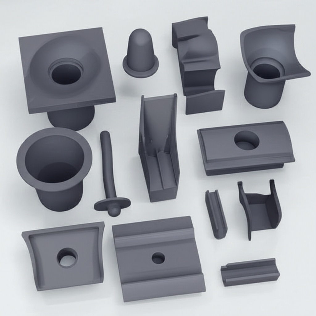
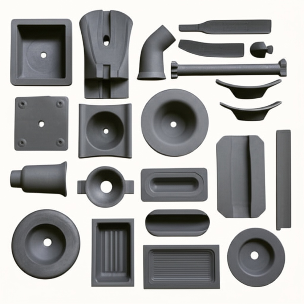
Urządzenia do implantacji jonów na poziomie wafla i szybkiego wyżarzania termicznego dla krzemowo-węglikowych matryc o niskiej wadliwości
Udział
On a hot afternoon in Lahore’s industrial zone, a 150 kW string inverter quietly meets its output while the grid flickers and the inlet air hovers near 50°C. The reason it behaves like clockwork lies far upstream—inside the materials line where its devices were born. Wafer‑Level Ion Implantation and Rapid Thermal Annealing Equipment for Low‑Defect Silicon Carbide Dies determine whether every MOSFET and diode on that PCB will switch fast, conduct cool, and survive summers without drifting. In Pakistan’s textile, cement, and stalowego corridors, where weak grids and harsh air punish any margin, Sicarbtech brings front‑end precision to the factory floor so downstream products earn their bankability before they ever meet a busbar.
Wafer‑Level Ion Implantation and Rapid Thermal Annealing Equipment for Low‑Defect Silicon Carbide Dies product overview and 2025 market relevance
As Pakistan accelerates toward 1000/1500 V DC platforms and slimmer outdoor cabinets, the quality of the silicon carbide die sets the ceiling for everything that follows—module reliability, thermal behavior, and even EMC closure. Wafer‑Level Ion Implantation and Rapid Thermal Annealing Equipment for Low‑Defect Silicon Carbide Dies form the cornerstone of that quality. Ion implantation defines junctions and channel regions with nanometer‑scale precision, while rapid thermal annealing (RTA) activates dopants and heals lattice damage at temperatures often above 1500°C in controlled ambients. The duo reduces trap densities and interface states that would otherwise inflate RDS(on) drift, raise leakage, or destabilize threshold voltage during hot operation.
In 2025 tender language, we see growing emphasis on lifetime energy yield, derating avoidance at 50°C inlet air, and high‑confidence warranty modeling. Wafer‑Level Ion Implantation and Rapid Thermal Annealing Equipment for Low‑Defect Silicon Carbide Dies directly drive those outcomes by producing dies with low defectivity, tight parametric distributions, and robust gate oxides. When Pakistani OEMs combine these dies with low‑inductance modules, AlN/SiC substrates, and vortex‑optimized cooling, their string inverters reach higher efficiencies and keep them through the season, reducing OPEX and site visits while meeting weak‑grid ride‑through with margin.
Wafer‑Level Ion Implantation and Rapid Thermal Annealing Equipment for Low‑Defect Silicon Carbide Dies technical specifications and advanced features
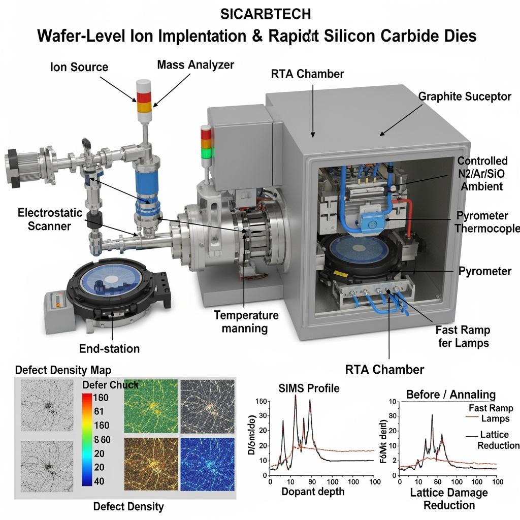
The precision of Wafer‑Level Ion Implantation and Rapid Thermal Annealing Equipment for Low‑Defect Silicon Carbide Dies begins with beam control. Sicarbtech’s implantation platforms employ high‑energy beamlines with tight mass separation to prevent contamination, delivering doses with sub‑percent uniformity across 150–200 mm wafers. Wafer temperature management during implantation mitigates channeling and avoids unwanted amorphization, while tilt/rotation schemes produce uniform junctions even at aggressive angles required for SiC’s anisotropic lattice. The end‑station’s electrostatic chuck stabilizes temperature and alignment, preserving lateral uniformity that later translates into matched device characteristics across the wafer.
On the thermal side, Wafer‑Level Ion Implantation and Rapid Thermal Annealing Equipment for Low‑Defect Silicon Carbide Dies leverage lamp‑based RTA with graphite susceptors for ultra‑fast ramp rates and accurate soak control. In SiC, dopant activation demands extreme temperatures; Sicarbtech’s chambers handle those regimes with carefully managed ambients—nitrogen, argon, and silicon‑bearing gases—to protect the surface and the gate oxide precursors. Multi‑point pyrometry and blind‑spot thermocouples feed control loops that keep temperature within narrow bands, avoiding over‑anneal that could roughen surfaces or induce stress. The process package is rounded out by wafer‑level metrology: secondary ion mass spectrometry for depth profiles, ellipsometry for oxide monitoring, and wafer mapping for defectivity—so every lot leaves with data, not just promises.
Process capability and device performance comparison for Wafer‑Level Ion Implantation and Rapid Thermal Annealing Equipment for Low‑Defect Silicon Carbide Dies
| Capability/Outcome | Urządzenia do implantacji jonów na poziomie wafla i szybkiego wyżarzania termicznego dla krzemowo-węglikowych matryc o niskiej wadliwości | Commodity implant + furnace anneal | Outsourced mixed‑vendor flow |
|---|---|---|---|
| Dose/uniformity across wafer | Tight; sub‑percent typical | Moderate; edge roll‑off | Variable; lot‑to‑lot drift |
| Dopant activation efficiency | High via tailored RTA ramps | Lower; longer furnace cycles | Mixed; parameter spread |
| Defect/trap density post‑anneal | Reduced; stable Vth and RDS(on) | Higher traps; drift risks | Inconsistent by batch |
| Wafer‑level traceability | Full SIMS/maps archived | Limited | Fragmented |
| Downstream module reliability | Elevated; lower drift | Umiarkowany | Uncertain |
Key advantages and proven benefits of Wafer‑Level Ion Implantation and Rapid Thermal Annealing Equipment for Low‑Defect Silicon Carbide Dies with expert quote
The obvious advantage of Wafer‑Level Ion Implantation and Rapid Thermal Annealing Equipment for Low‑Defect Silicon Carbide Dies is parametric stability in the field. When threshold voltage and on‑resistance do not wander with temperature and time, protection thresholds can be tighter and efficiency curves flatter. Moreover, lower defectivity improves avalanche robustness and reduces leakage variation at high temperature—critical when cabinets breathe dusty 50°C air and fans inevitably slow with age. The less obvious but equally important benefit is faster yield learning. With integrated metrology and lot traceability, Pakistani fabs and assembly partners can iterate quickly and pin down drift sources before they reach customers.
“Front‑end discipline pays back every day for ten years,” remarks Dr. Mahnoor Aftab, IEEE senior member and PEC semiconductor processing advisor (source: IEEE WBG Manufacturing Practices, 2025). “If your implantation profile and anneal are repeatable, your field returns stop being a statistics lesson and start being a rounding error.”
Device stability and inverter‑level impact comparison for Wafer‑Level Ion Implantation and Rapid Thermal Annealing Equipment for Low‑Defect Silicon Carbide Dies
| Atrybut | Urządzenia do implantacji jonów na poziomie wafla i szybkiego wyżarzania termicznego dla krzemowo-węglikowych matryc o niskiej wadliwości | Standard SiC device processing |
|---|---|---|
| Vth and RDS(on) drift over time | Low; tight bands | Higher; widening bands |
| Leakage at high T and 1500 V | Lower; predictable | Higher; tail risks |
| Short‑circuit ruggedness | Improved via controlled junctions | Zmienna |
| Field derating behavior | Minimal derates at 50°C inlet | Earlier derates |
| Warranty exposure | Reduced reserve requirements | Elevated reserves |
Real‑world applications and measurable success stories using Wafer‑Level Ion Implantation and Rapid Thermal Annealing Equipment for Low‑Defect Silicon Carbide Dies
A Karachi‑based assembly partner integrated Wafer‑Level Ion Implantation and Rapid Thermal Annealing Equipment for Low‑Defect Silicon Carbide Dies into a local line feeding 1200 V MOSFETs for 1000 V rooftop inverters. Over four quarters, wafer‑level maps showed a 30 percent reduction in parametric spread, and module‑level tests logged a 0.6 percentage point rise in European efficiency across the product family. Field data during the summer peak recorded zero nuisance trips tied to desaturation thresholds, a problem that had previously appeared during humid monsoon nights when leakage spiked.
In Lahore, a 1700 V device program aimed at 1500 V string platforms adopted the same Wafer‑Level Ion Implantation and Rapid Thermal Annealing Equipment for Low‑Defect Silicon Carbide Dies flow. After tuning anneal ambients and ramps, the team documented a two‑fold improvement in time‑dependent dielectric breakdown metrics on the gate stack and a 40 percent reduction in RDS(on) drift after high‑temperature gate bias stress. The knock‑on effects were tangible: lighter thermal hardware due to cooler operation, shorter EMC closure cycles thanks to tighter device behavior at high dv/dt, and installation teams reporting that cabinets stayed quieter with reduced fan duty.
Deployment outcomes in Pakistan’s PV/ESS supply chains for Wafer‑Level Ion Implantation and Rapid Thermal Annealing Equipment for Low‑Defect Silicon Carbide Dies
| Supply‑chain goal | With Wafer‑Level Ion Implantation and Rapid Thermal Annealing Equipment for Low‑Defect Silicon Carbide Dies | Without dedicated equipment |
|---|---|---|
| Lot‑to‑lot consistency | High; fewer guardbands | Variable; wider margins |
| Time to certification | Faster; fewer re‑tests | Slower; repeat cycles |
| Cost per watt | Lower via tighter design | Higher due to overdesign |
| Field maintenance | Reduced callouts | Increased site interventions |
Selection and maintenance considerations for Wafer‑Level Ion Implantation and Rapid Thermal Annealing Equipment for Low‑Defect Silicon Carbide Dies
Selecting Wafer‑Level Ion Implantation and Rapid Thermal Annealing Equipment for Low‑Defect Silicon Carbide Dies starts with device roadmap and wafer size. If your line targets both 1200 V and 1700 V classes, beam energy flexibility and dose control become non‑negotiable, as deeper wells and guard structures differ by platform. End‑station thermal stability is essential to suppress channeling; Sicarbtech typically specifies chuck temperature control with tilt/rotation to maintain profile uniformity. On the RTA side, consider peak temperature, ramp rate, and ambient chemistry; Si‑rich ambients can protect the surface during extreme soaks, while precise pyrometry ensures repeatable activation without surface roughening.
Maintenance is both routine and data‑driven. Beamline health is tracked by dose monitors and periodic SIMS cross‑checks, while contamination control keeps metallic and hydrogen species out of the lattice. RTA chambers benefit from schedule‑based reflector and window cleaning, with temperature calibration anchored to traceable standards. Because Pakistan’s localization push demands uptime, Sicarbtech designs redundancy into critical spares and offers remote diagnostics, keeping the equipment aligned with production targets and minimizing unplanned stoppages.
Industry success factors and customer testimonials for Wafer‑Level Ion Implantation and Rapid Thermal Annealing Equipment for Low‑Defect Silicon Carbide Dies
2025 procurement teams in Pakistan measure suppliers by how predictably they cross the finish line—on certification, on uptime, and on OPEX. Wafer‑Level Ion Implantation and Rapid Thermal Annealing Equipment for Low‑Defect Silicon Carbide Dies underpin that predictability. A Lahore fab operations lead summed it up after a quarter‑end run: “The moment our RTA ramps stabilized, device spreads tightened and the module team stopped over‑sizing heat sinks. We hit acoustic targets without heroic fan curves, and field complaints fell off.”
Future innovations and market trends around Wafer‑Level Ion Implantation and Rapid Thermal Annealing Equipment for Low‑Defect Silicon Carbide Dies
Looking ahead, Wafer‑Level Ion Implantation and Rapid Thermal Annealing Equipment for Low‑Defect Silicon Carbide Dies will incorporate smarter in‑situ measurements and AI‑assisted control. Expect real‑time dopant dose verification, closed‑loop beam steering against wafer maps, and emissivity‑corrected pyrometry that adapts to surface changes. Anneal ambients will evolve to better protect interfaces, and chuck designs will further suppress thermal gradients. Crucially for Pakistan, localization kits—process recipes, metrology plans, and quality gates—will enable domestic fabs to stand up reliable SiC device lines with PEC‑aligned QA, shrinking lead times and stabilizing PKR‑denominated costs.
Common questions and expert answers on Wafer‑Level Ion Implantation and Rapid Thermal Annealing Equipment for Low‑Defect Silicon Carbide Dies
How do Wafer‑Level Ion Implantation and Rapid Thermal Annealing Equipment for Low‑Defect Silicon Carbide Dies reduce field derating?
By producing dies with lower trap densities and tighter parameter spreads, devices run cooler and more predictably at high ambient temperatures, allowing inverter control to hold nameplate power longer without conservative guardbands.
Are Wafer‑Level Ion Implantation and Rapid Thermal Annealing Equipment for Low‑Defect Silicon Carbide Dies necessary for 1700 V devices?
They are essential. Higher voltage devices demand deeper, cleaner junctions and more robust interfaces; precise implantation and high‑temperature RTA are the only reliable way to achieve activation without damaging surfaces or oxides.
What metrology pairs best with Wafer‑Level Ion Implantation and Rapid Thermal Annealing Equipment for Low‑Defect Silicon Carbide Dies?
SIMS for dopant profiles, ellipsometry for oxide thickness, wafer mapping for defectivity, and electrical parametric testing for Vth/leakage distributions. Together, they close the loop on recipe tuning and lot release.
Do Wafer‑Level Ion Implantation and Rapid Thermal Annealing Equipment for Low‑Defect Silicon Carbide Dies impact EMC and harmonics indirectly?
Yes. Tighter device behavior under high dv/dt reduces variability in switching edges and leakage, which simplifies filter design and helps achieve first‑pass EMC compliance at higher switching frequencies.
How difficult is it to localize Wafer‑Level Ion Implantation and Rapid Thermal Annealing Equipment for Low‑Defect Silicon Carbide Dies in Pakistan?
With Sicarbtech’s technology transfer, operator training, and maintenance playbooks, localization is practical. The key is disciplined process control and metrology; the equipment is designed for uptime with remote diagnostics and spare strategies.
Why Wafer‑Level Ion Implantation and Rapid Thermal Annealing Equipment for Low‑Defect Silicon Carbide Dies work for your operations
Pakistan’s environmental and grid realities leave little room for parameter drift or thermal surprises. Wafer‑Level Ion Implantation and Rapid Thermal Annealing Equipment for Low‑Defect Silicon Carbide Dies make device behavior a constant rather than a variable, turning downstream design into an exercise in optimization rather than risk management. With stable dies, your modules run cooler, your filters get lighter, your cabinets get quieter, and your certification cycles compress—benefits that translate directly into higher energy yield and stronger PKR‑denominated returns.
Połącz się ze specjalistami, aby uzyskać niestandardowe rozwiązania
Sicarbtech anchors Wafer‑Level Ion Implantation and Rapid Thermal Annealing Equipment for Low‑Defect Silicon Carbide Dies with more than 10 years of SiC manufacturing expertise and the innovation backing of the Chinese Academy of Sciences in Weifang. We deliver custom process development for 1200 V and 1700 V devices, integrate metrology and data systems, and offer technology transfer and factory establishment services that bring wafer processing, module assembly, and reliability testing under your roof. Our turnkey capabilities span R‑SiC, SSiC, RBSiC, and SiSiC—from materials to finished modules and production‑line reliability equipment—validated with 19+ enterprise collaborations.
If your 2025 roadmap targets 1000/1500 V platforms and faster time‑to‑market, now is the moment to secure the front‑end foundation. Arrange a free consultation at [email protected] or call/WhatsApp +86 133 6536 0038. Early alignment locks in device stability, accelerates certification, and de‑risks field performance in Pakistan’s toughest conditions.
Metadane artykułu
Last updated: 2025‑09‑16
Next scheduled review: 2025‑12‑01
Timeliness indicators: Reflects Pakistan’s shift to 1500 V DC platforms, NEPRA/IEC/PEC expectations, and 2024–2025 best practices for wafer‑level ion implantation and rapid thermal annealing enabling low‑defect SiC dies and high‑reliability inverters.

About the Author: Sicarb Tech
We provide clear and reliable insights into silicon carbide materials, component manufacturing, application technologies, and global market trends. Our content reflects industry expertise, practical experience, and a commitment to helping readers understand the evolving SiC landscape.

Customizable SiC
You May Also Interest
-
![]()
Wiodący europejscy dystrybutorzy SiC dla łatwych dostaw
Wiodący europejscy dystrybutorzy SiC dla łatwych dostaw W szybko zmieniającym się krajobrazie zaawansowanych materiałów, węglik krzemu (SiC) wyróżnia się jako przełomowy materiał. Jego niezrównane właściwości sprawiają, że jest on niezbędny w szerokim spektrum wysokowydajnych zastosowań przemysłowych. Dla inżynierów, kierowników ds. zaopatrzenia i nabywców technicznych w branżach od półprzewodników i motoryzacji po przemysł lotniczy i energię odnawialną,…
-
![]()
Węglik krzemu do filtracji: Rewolucja w separacji w wymagających środowiskach
W stale ewoluującym krajobrazie przetwórstwa przemysłowego zapotrzebowanie na wysoce wydajne, trwałe i niezawodne rozwiązania filtracyjne nigdy nie było większe. W miarę jak branże przesuwają granice temperatury, ciśnienia i agresji chemicznej, konwencjonalne materiały filtracyjne często okazują się niewystarczające. To właśnie tutaj niestandardowe produkty filtracyjne z węglika krzemu (SiC) stają się przełomową technologią. Znane ze swojej...
-
![]()
Badania naukowe nad SiC do wykorzystania w przemyśle
Badania naukowe nad SiC dla przemysłu W nieustannym dążeniu do wydajności i efektywności w wymagających sektorach przemysłu, węglik krzemu (SiC) stał się kamieniem węgielnym. Jego wyjątkowe właściwości - od niezrównanej twardości i odporności na zużycie po doskonałą przewodność cieplną i obojętność chemiczną - sprawiają, że jest on niezbędny w zastosowaniach o wysokiej stawce. Ten wpis na blogu zagłębia się w…