Custom SiC Substrates and Wafers for Electronics Manufacturers
Udział
Sicarbtech — Silicon Carbide Solutions Expert. Based in Weifang City, China’s silicon carbide manufacturing hub and a member of the Chinese Academy of Sciences (Weifang) Innovation Park, we help Pakistan’s emerging semiconductor ecosystem procure and qualify custom SiC substrates and wafers for power electronics and RF devices. With 10+ years of advanced SiC experience and successful collaborations with 19+ enterprises, Sicarbtech delivers full‑cycle support—from boule growth and wafering to epi, metrology, packaging, and technology transfer for localized capability.
Executive Summary: 2025 Outlook for SiC Wafers and Substrates in Pakistan
Pakistan’s industrial transition toward electrification, efficient motor drives, and grid resilience is placing power electronics at the center of investment plans. As textile mills upgrade variable‑speed drives, cement plants optimize kilns and baghouses, and stalowego producers modernize furnaces and auxiliary loads, the demand for high‑efficiency power conversion rises. In this context, silicon carbide wafers—especially 4H‑SiC and 6H‑SiC—are moving from niche imports to strategic components for local OEMs and research institutions. Lower switching losses, higher breakdown fields, and excellent thermal conductivity translate into smaller, more efficient inverters, rectifiers, and high‑temperature modules—advantages that are echoed in backup power, solar inverters, EV charging, and industrial motor control across Punjab and Sindh.
Furthermore, the procurement landscape is changing. ISO 9001/14001/45001 frameworks are spreading among export‑linked manufacturers, while PSQCA‑referenced conformity and insurer‑requested reliability evidence are becoming familiar in tenders. Currency volatility and long logistics legs push buyers to seek predictable lead times, tight quality controls, and PKR‑denominated ROI models. Building on this, Sicarbtech integrates custom SiC wafer specifications, epi options, device‑oriented metrology, and documentation that stands up to buyer audits—so engineering leaders can justify design wins and operations can plan around reliable deliveries. The 2025 outlook favors partners who combine materials expertise, device‑level understanding, and scalable supply.
Industry Challenges and Pain Points in Pakistan’s Semiconductor Procurement
Local device development teams face a steep hill. On paper, importing SiC wafers is straightforward; in practice, the challenges multiply. Engineering needs crystal quality—low micropipe density, controlled basal plane dislocation levels, stable off‑axis cuts for epitaxy; operations need predictable yield through wafering and polishing; finance needs cost visibility in PKR; and compliance teams need documentation aligned with ISO systems and PSQCA references. When any of these fail, the entire project timeline slips.
Pakistan’s industrial users amplify the urgency. Textile mills adopting high‑efficiency drives want inverters that run cooler in dusty, high‑ambient conditions, with fewer failures during power disturbances. Cement plants seek robust rectifiers and high‑temperature gate drives for kiln auxiliaries. Steel producers want compact, reliable converters for high‑current applications. Yet device OEMs struggle when wafer flatness, bow, or surface roughness cause epi defects; when doping uniformity across a lot varies; or when miscut angles drift outside the tight windows required for step‑flow epitaxy. “Every uncontrolled defect you allow into the front end reappears as a costly yield loss at the back end,” notes Engr. Faraz Khan, a reliability auditor who supports industrial electronics programs across Punjab (South Asia Reliability Insights, 2024).
Logistics adds friction. Lead times that were eight to ten weeks can stretch unexpectedly; air freight for urgent lots becomes expensive; and customs clerance delays play havoc with pilot runs. Currency fluctuations complicate budgets, forcing design teams to freeze specs earlier than they’d like. Compliance expectations also rise as export customers ask for traceable materials, environmental documentation, and robust ESD and cleanliness controls. “Documentation is not bureaucracy—it is the scaffolding that keeps quality stable across time and teams,” says Dr. Nadia Rahman, EHS advisor to multiple OEM clusters (EHS & Industry Review, 2024). In contrast, opportunistic sourcing—spot buys without metrology, mixed wafer origins, incomplete COAs—produces uneven device performance, missed qualification gates, and strained customer relationships.
Moreover, many local teams are transitioning from silicon to SiC. Process conditions that were forgiving on Si (e.g., higher defect tolerance, wider thermal budgets) can be unforgiving on SiC. Without application‑aware guidance on wafer grade, off‑axis angles, epi thickness/doping, and surface preparation, fabs and university lines burn time discovering avoidable pitfalls. “Reliability is engineered, not purchased off a catalog,” adds Prof. Liu, a materials scientist associated with the Chinese Academy of Sciences (Materials Engineering Commentaries, 2024). For 2025, the winning model couples stable wafer supply with device‑level process intelligence and audit‑ready documentation.
Sicarbtech’s Silicon Carbide Solutions Portfolio for Device Manufacturers
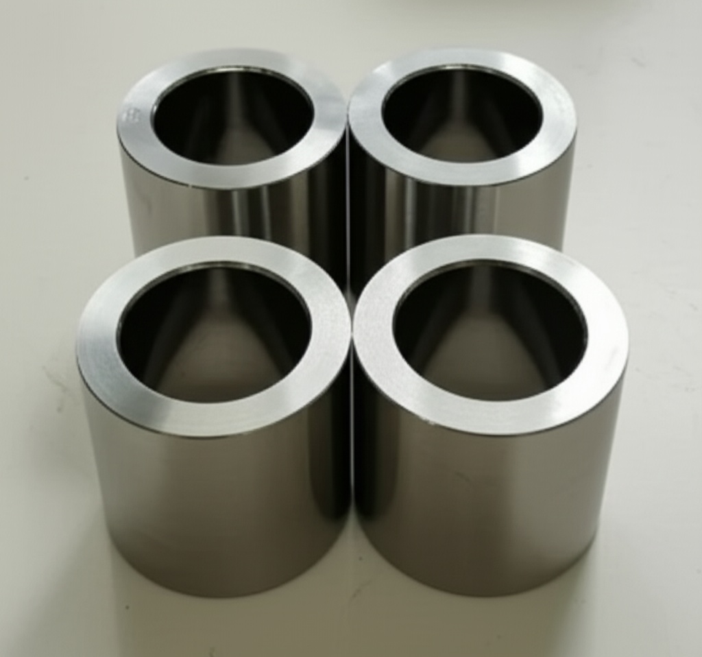
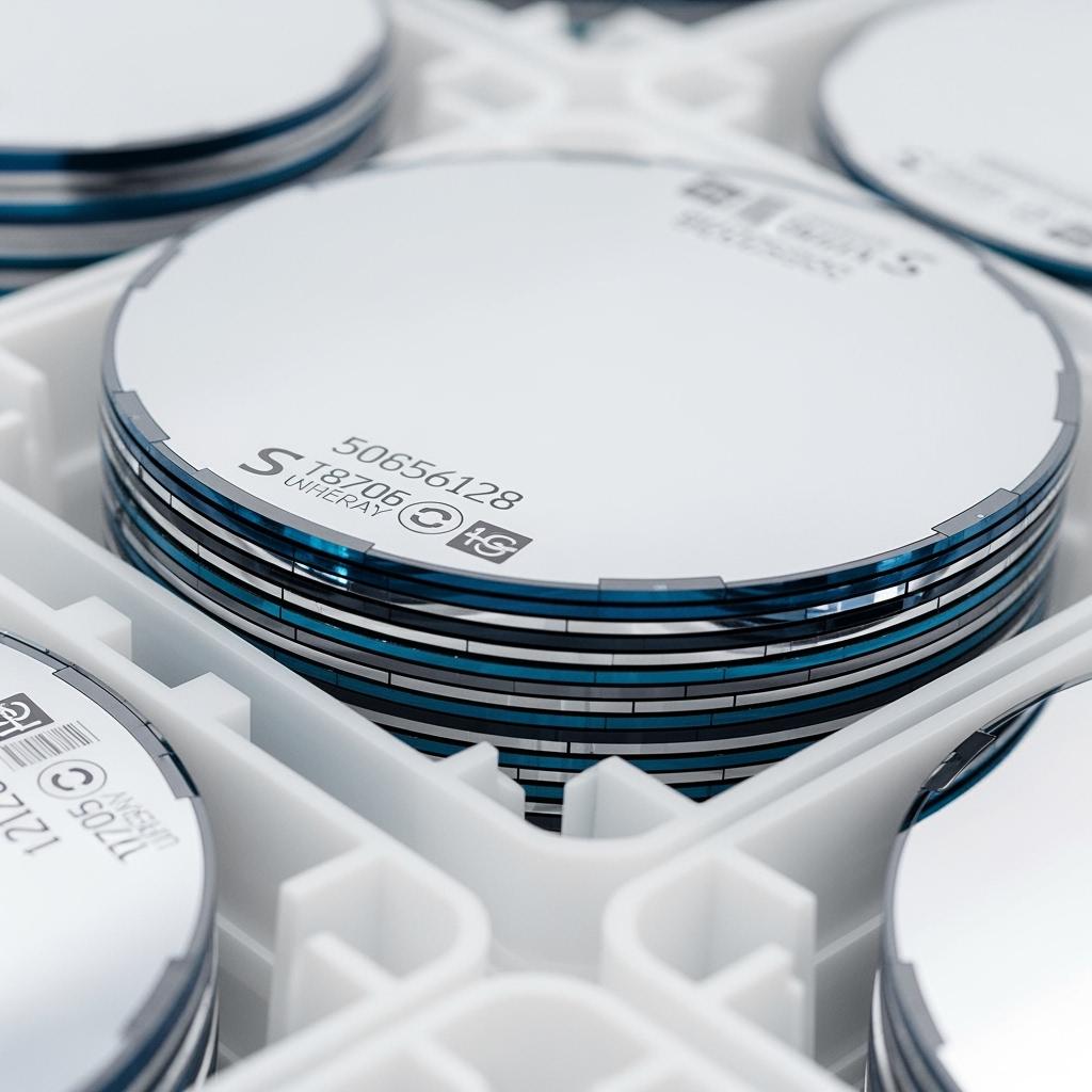
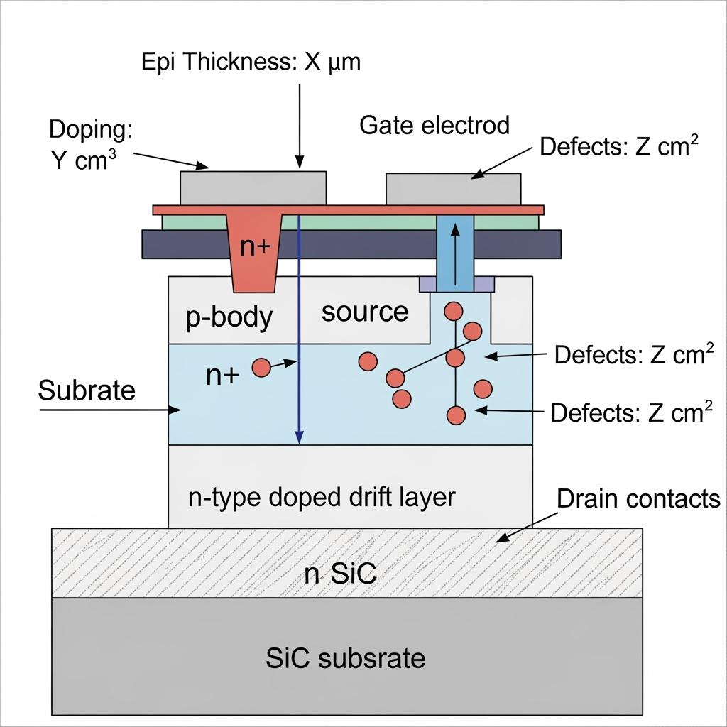
Sicarbtech supplies 4H‑SiC and 6H‑SiC substrates and wafers tailored to device intent—MOSFETs, IGBTs and diodes, Schottky barrier diodes, JFETs, and RF power devices. For power electronics, 4H‑SiC dominates due to its superior electron mobility and breakdown characteristics; we offer n‑type and semi‑insulating options, with standard diameters from 100 mm to 200 mm and development access to larger formats as roadmaps evolve. Off‑cut angles (commonly 4° toward <11‑20>) are controlled for step‑flow during epitaxy, while defect metrics—micropipe density, threading dislocations, basal plane dislocations—are specified per device sensitivity.
For epitaxial growth, we deliver drift layers with tight thickness and doping control matched to target breakdown voltages—650 V to 6.5 kV and beyond—alongside buffer layers engineered for trap minimization. Surface preparation and polishing meet epi‑ready standards with low total thickness variation (TTV) and low roughness (e.g., Ra in sub‑angstrom ranges on epi‑ready faces). We bundle metrology—AFM, XRD rocking curves, Nomarski inspection, micropipe/BPD maps—and electrical tests (CV/IV on test structures where applicable) with each lot. For RF and high‑frequency designs, semi‑insulating 4H‑SiC offers low loss and high thermal conductivity, supporting compact, thermally efficient MMICs and power amplifiers.
Beyond wafers, Sicarbtech supports module‑level ambitions. We advise on die attach and metallization compatibility, high‑temperature packaging, and thermal interface choices that exploit SiC’s conductivity. For Pakistani OEMs building industrial inverters or chargers, we can align wafer specs with available epi providers and package houses, streamlining the journey from substrate to module. Documentation aligns with ISO 9001/14001/45001 and PSQCA references; for OEM/ODM programs, we prepare IATF 16949‑aligned control plans and PPAP‑style evidence to accelerate qualification.
Technical Comparison: SiC vs Traditional Silicon for Power Devices
Key material parameters that drive device performance and reliability
| Parameter (typical) | 4H‑SiC | 6H‑SiC | Silicon |
|---|---|---|---|
| Bandgap (eV) | ~3.26 | ~3.0 | ~1.12 |
| Critical electric field (MV/cm) | ~2.5–3.0 | ~2.0–2.5 | ~0.3 |
| Thermal conductivity (W/m·K) | ~370–490 (orientation/temp dependent) | ~370–490 | ~150 |
| Electron mobility (cm²/V·s) | ~800–1,000 (bulk; channel lower) | ~400–600 | ~1,400 (bulk) |
| Breakdown voltage per thickness | Bardzo wysoka | Wysoki | Niski |
| Max junction temperature (°C, device‑level limit) | 175–200+ (package dependent) | 175–200+ | 150–175 |
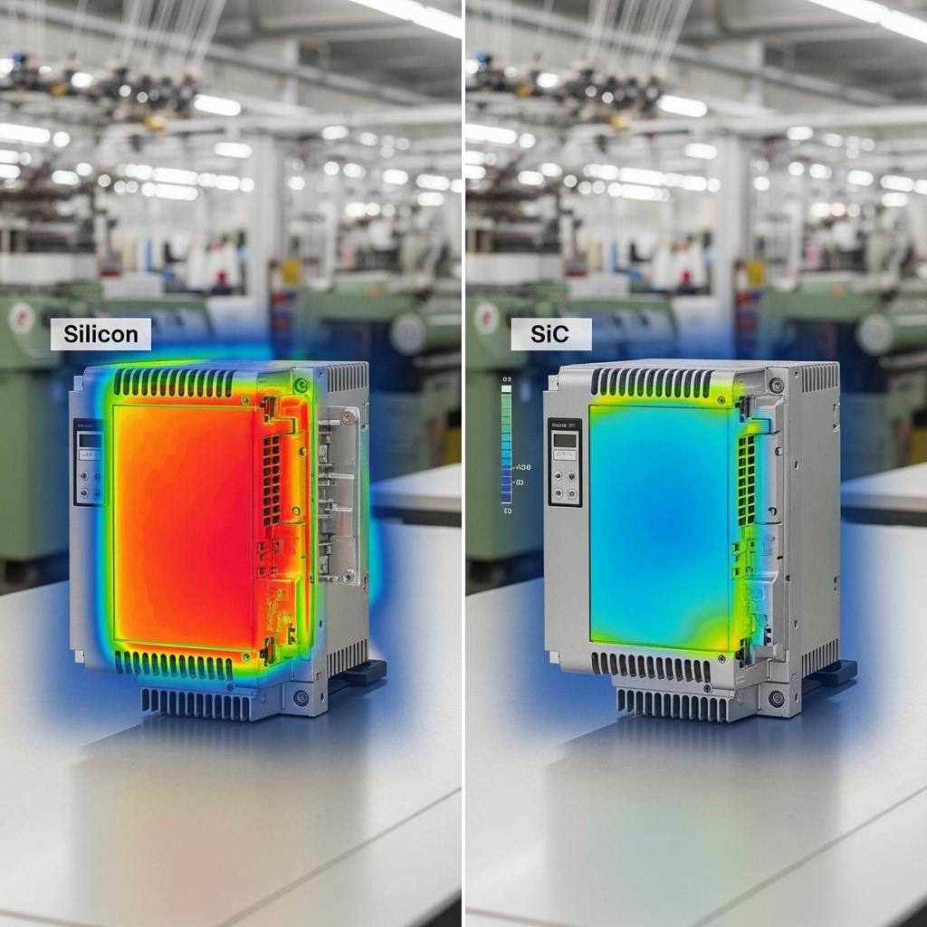
The combination of higher breakdown field and strong thermal conductivity enables thinner drift layers, lower losses, and higher power density—features that directly benefit inverters, chargers, and high‑temperature controls used across Pakistani industrial sites.
Wafer specification ranges aligned with common device targets
| Device class | Średnica | Off‑cut | Conductivity type | Epi thickness (µm) | Net doping (cm⁻³) | Uwagi |
|---|---|---|---|---|---|---|
| 650–1,200 V MOSFET/SBD | 150/200 mm | 4° toward <11‑20> | n‑type substrate | 8–15 | 5e15–2e16 | Low BPD epi, tight TTV |
| 1.7–3.3 kV MOSFET/IGBT/diode | 150/200 mm | 4° toward <11‑20> | n‑type substrate | 20–40 | 5e14–2e15 | Uniform lifetime control |
| 3.3–6.5 kV diode/thyristor | 100/150 mm | 4° toward <11‑20> | n‑type substrate | 50–100 | 1e14–5e14 | Thick epi, trap management |
| RF/MMIC (semi‑insulating) | 100/150 mm | On‑axis or low off‑cut | Semi‑insulating | — | — | Low loss, high resistivity |
These ranges are illustrative; specific lots are engineered after device modeling, lifetime targets, and epi provider capabilities are aligned.
Comparative device‑level outcomes in industrial use cases
| Industrial application in Pakistan | Silicon device baseline | SiC device outcome | System‑level impact |
|---|---|---|---|
| Textile mill VFDs (dusty, high ambient) | Si IGBT inverter | SiC MOSFET/SBD inverter | 1–3% higher system efficiency; smaller heatsinks; improved uptime |
| Cement kiln auxiliaries and baghouses | Si IGBT rectifier/drive | SiC diode + MOSFET | Higher temp resilience; fewer trips during sags; tighter speed control |
| Steel reheat furnace controls | Si IGBT | SiC MOSFET | Faster switching, better PF; reduced cabinet cooling load |
| Solar + storage for estates | Si IGBT inverter | SiC inverter | Higher power density; better partial‑load efficiency |
Efficiency improvements and thermal headroom often allow enclosure downsizing and simpler cooling—valuable advantages where ambient temperatures and dust are persistent realities.
Real‑World Applications and Success Stories from Regional Projects
A Lahore‑area controls OEM developing 50–90 kW VFDs for textile mills struggled with overheating at high ambient temperatures. Sicarbtech supplied 150 mm 4H‑SiC n‑type wafers with epi targeted for 1,200 V MOSFET designs, paired with process guidance on channel mobility and interface traps. Prototype inverters demonstrated a measurable efficiency gain at partial load and allowed a 20–30% reduction in heatsink mass. Field trials reported cooler cabinets and fewer thermal derates during peak summer operation.
In a Karachi industrial estate piloting fast DC chargers for logistics fleets, the integrator needed compact rectifier stages with high thermal resilience. We delivered semi‑insulating 4H‑SiC substrates and coordinated with an epi partner for low‑defect layers. The resulting power modules supported denser layouts and maintained performance over extended duty cycles. “Quality follows stability,” remarks Engr. S. Aftab, a reliability consultant to several OEMs (Pakistan Maintenance & Reliability Exchange, 2024). “When your material inputs are controlled and your documentation is tight, you spend more time optimizing and less time firefighting.”
A university‑industry lab in Islamabad required mixed lots—MOSFET‑oriented wafers and RF‑friendly semi‑insulating substrates—for device research. Sicarbtech staged deliveries to match grant milestones, provided full metrology packs, and trained staff on handling and cleaning to reduce particle‑induced defects. The lab accelerated its learning curve, meeting review deadlines and securing follow‑on funding.
Technical Advantages and Implementation Benefits with Local Regulatory Compliance
Silicon carbide’s wide bandgap, high breakdown field, and superior thermal conductivity are not academic talking points—they translate into practical resilience in Pakistan’s environments. Devices run cooler, switch faster, and tolerate higher junction temperatures. For integrators, that means smaller magnetics, reduced cooling overhead, and cabinets that handle high ambient conditions without derating. Additionally, lower conduction and switching losses boost energy efficiency in estates where electricity costs and power quality both challenge operations.
Sicarbtech embeds compliance into engineering from day one. We supply PSQCA‑referenced conformity packs, ISO 9001/14001/45001 documentation, and, for OEM/ODM programs, IATF 16949‑aligned control plans and PPAP‑style evidence. Our metrology reports—BPD/micropipe maps, AFM roughness, XRD rocking curves, TTV, bow, and warp—simplify buyer and insurer audits. EHS guidance covers cleanroom handling, solvent management, and ESD controls, helping local lines align with best practice. “Compliance is a design constraint, not an afterthought,” emphasizes Dr. Li, CAS‑affiliated materials scientist (CAS Industry Notes, 2024). By designing for documentation, qualification gates move faster and risks shrink.
Custom Manufacturing and Technology Transfer Services by Sicarbtech
Sicarbtech’s competitive advantage is a turnkey model that spans crystal growth, wafering, polishing, epi integration, and knowledge transfer—backed by the Chinese Academy of Sciences (Weifang) Innovation Park.
We source or grow 4H/6H boules according to device targets, control off‑axis cuts for epitaxy, and slice, lap, and polish to strict flatness and TTV. Proprietary polishing workflows deliver epi‑ready surfaces with sub‑angstrom roughness, while edge profiles and bevels are tuned for downstream handling. For epi, we coordinate drift and buffer layers with tight thickness and doping windows, integrate lifetime control where required, and validate with full metrology. Electrical test structures can be included for CV/IV sampling. Throughout, batch traceability links every wafer to boule and process history.
For localization, we offer complete technology transfer packages. These include process know‑how from boule handling and wafering through cleaning and packaging; equipment specifications for wire saws, double‑siders, CMP, cleaning tools, metrology (AFM, XRD, optical inspection), and ESD infrastructure; and training programs for operators, process engineers, QC, and maintenance. Factory establishment services cover feasibility studies, cleanroom design (ISO class targets), utilities and HVAC, EHS alignment with Pakistani regulations, and line commissioning. Hybrid models stage critical steps near growth centers while wafer cleaning, metrology, and kitting occur locally—shortening lead times, reducing FX exposure, and building domestic capability.
Quality control and certification support are integral. Statistical process control monitors TTV, bow/warp, Ra, epi thickness/doping, defect maps, and yield. We prepare control plans and capability studies, support MSA where needed, and bundle documentation to ease audits. After launch, our engineers remain engaged—tuning CMP parameters, refining epi recipes with partners, and feeding field data back into specifications. Over a decade and 19+ enterprise partnerships, this comprehensive, transferable approach has delivered faster qualifications, fewer first‑run issues, and clear PKR‑based ROI.
Future Market Opportunities and 2025+ Trends in SiC for Pakistan
Several forces will accelerate SiC adoption beyond 2025. Industrial electrification will expand with motor drive retrofits in textiles and continuous process optimization in cement and steel. Distributed energy and backup power will grow as estates pursue resilience, pushing demand for compact, efficient inverters and rectifiers. EV charging pilots and fleet electrification will require high‑power converters with robust thermal behavior. On the supply side, localized finishing and metrology will shorten lead times and tame currency risk, while export buyers will increase traceability demands—favoring suppliers who can provide wafer‑to‑module documentation.
Moreover, the research base is maturing. University labs are moving from device demonstrators to reliability studies—gate oxide integrity, short‑circuit robustness, and cosmic‑ray‑induced failure rates—which will feed into industrial designs. As this ecosystem strengthens, the case for consistent wafer quality, reliable epi partnerships, and rigorous metrology becomes even more compelling. In short, SiC is shifting from a tactical performance upgrade to a strategic foundation for Pakistan’s efficient, resilient industrial power.
Często zadawane pytania
Which wafer grade—4H‑SiC or 6H‑SiC—should I choose for my device?
For most power electronics (MOSFETs, SBDs, IGBTs, high‑voltage diodes), 4H‑SiC is preferred thanks to superior electron mobility and high critical field. 6H‑SiC sees use in certain RF or legacy processes but is less common for modern power devices. We finalize selection after reviewing device physics, switching frequency, and breakdown targets.
How tight are your epi tolerances for industrial power devices?
Typical drift layers span 8–100 µm with net doping windows from ~1e14 to 2e16 cm⁻³, depending on voltage class. Thickness uniformity and TTV targets are set per device. We provide full metrology—thickness maps, SIMS on request, and defect mapping—so you can correlate device yields to incoming material.
Can you support PPAP‑style documentation and IATF 16949 expectations?
Yes. We prepare control plans, capability studies, MSA where appropriate, and PPAP‑style submission packs aligned with automotive and industrial OEM requirements. Our ISO 9001/14001/45001 documentation and PSQCA‑referenced conformity help speed tenders and audits.
What lead times should Pakistani buyers expect for custom wafers?
Standard lots typically run 6–12 weeks depending on diameter, off‑cut, epi thickness/doping, and volume. We coordinate phased deliveries and can stage metrology and kitting locally under technology transfer arrangements to shorten effective lead times.
How do you help first‑time SiC device teams reduce risk?
We align wafer specs with your device models, recommend epi stack parameters, and share handling/cleaning SOPs to protect surfaces. We also provide failure‑analysis pathways and link metrology with device outcomes, so you can troubleshoot quickly during pilot runs.
Can Sicarbtech arrange private label and custom marking?
Yes. We support private label, laser marking with lot and wafer ID conventions, and packaging tailored to your cleanroom flow. Documentation maps IDs to boule and process history for full traceability.
What shipping and customs support do you provide into Pakistan?
We prepare HS classifications, moisture/ESD‑safe packaging, and documentation to streamline customs. For critical programs, we can pre‑position safety stock or buffer lots, and we synchronize shipments with your pilot or ramp schedule.
Do you supply semi‑insulating SiC for RF and high‑frequency applications?
Yes. Semi‑insulating 4H‑SiC substrates are available with high resistivity and low loss, suitable for RF power and MMIC applications. We coordinate with epi partners for GaN‑on‑SiC or related stacks where applicable.
How do you ensure batch‑to‑batch consistency in wafer quality?
SPC on TTV, bow/warp, Ra, BPD/micropipe counts; epi thickness/doping maps; and electrical sampling on test structures. We maintain full traceability from boule to wafer and provide comprehensive COAs with each lot.
Can you support local capability building for wafer finishing and metrology?
Absolutely. Through technology transfer, we define equipment lists, SOPs, cleanroom design, and training to establish local cleaning, metrology, and kitting—reducing lead times and FX exposure while growing domestic skills.
Dokonywanie właściwego wyboru dla swoich operacji
Selecting SiC substrates and wafers is more than a purchasing decision; it is a strategic commitment to efficiency, thermal resilience, and product leadership. Sicarbtech’s integrated model—custom wafer specifications, disciplined epi partnerships, deep metrology, audit‑ready documentation, and technology transfer—gives Pakistani device makers a reliable path from concept to qualified production. Whether you are building a 1,200 V industrial inverter, a high‑power charger, or a research platform for next‑generation devices, the right SiC foundation accelerates every step that follows.
Konsultacje ekspertów i niestandardowe rozwiązania
Share your device targets, breakdown voltages, switching frequencies, and packaging constraints with Sicarbtech’s engineering team. We will propose the optimal wafer grade, off‑cut, epi stack, and metrology plan, then map an implementation schedule synchronized with your tape‑out and pilot runs—complete with a PKR‑based ROI model. Contact: [email protected] or +86 133 6536 0038.
Explore Related Cluster Resources
- Benefits of SiC Wafers in Power and RF Electronics
- Why Silicon Carbide Substrates Are Ideal for High Voltage Devices
- Custom SiC Wafer Specifications for Semiconductor Applications
- Tailored Silicon Carbide Substrates for Device Manufacturers
- 4H and 6H SiC Wafer Grades for High-Performance Electronics
- Epitaxial Growth Options for Custom SiC Wafers
- OEM and ODM Services for Custom SiC Wafer Production
- Private Label and Custom Marking for SiC Substrates
- Use Cases of SiC Substrates in IGBT and MOSFET Fabrication
- Procurement and Shipping Guide for SiC Wafers to Pakistan
Metadane artykułu
Last updated: 2025-09-23
Następny planowany przegląd: 2026-01-15
Content freshness indicators: 2025 Pakistan semiconductor outlook integrated; PSQCA and ISO 9001/14001/45001 considerations reflected; IATF 16949 support for OEM/ODM programs; ROI framed in PKR; case insights from 2023–2025 Sicarbtech engagements; trends aligned with electrification, grid resilience, and localization initiatives.

About the Author: Sicarb Tech
We provide clear and reliable insights into silicon carbide materials, component manufacturing, application technologies, and global market trends. Our content reflects industry expertise, practical experience, and a commitment to helping readers understand the evolving SiC landscape.

Customizable SiC
You May Also Interest
-
![]()
-
![]()
Wydajna logistyka SiC dla globalnego zasięgu materiałowego
Wydajna logistyka SiC dla globalnego zasięgu materiałowego We współczesnym, szybko rozwijającym się krajobrazie przemysłowym zapotrzebowanie na zaawansowane materiały, takie jak węglik krzemu (SiC), gwałtownie rośnie w wielu sektorach. Od zasilania nowej generacji pojazdów elektrycznych po umożliwianie przetwarzania w wysokich temperaturach w piecach przemysłowych, niestandardowe produkty z węglika krzemu okazują się niezbędne. Ale w jaki sposób te krytyczne…
-
![]()
Globalne usługi eksportu SiC uproszczone i niezawodne
Global SiC Export Services Made Simple & Reliable In today’s rapidly advancing industrial landscape, the demand for high-performance materials is paramount. Among these, silicon carbide (SiC) stands out as a critical material, essential for pushing the boundaries of various high-temperature, abrasive, and corrosive environments. For engineers, procurement managers, and technical buyers across diverse sectors, sourcing…