Next-Gen SiC Wafers for Power Electronics Excellence
Share
Next-Gen SiC Wafers for Power Electronics Excellence
Introduction: The Pivotal Role of SiC Wafers in Modern Power Electronics
The relentless pursuit of higher efficiency, increased power density, and superior performance in power electronic systems has spotlighted silicon carbide (SiC) as a transformative material. SiC wafers, the foundational substrates for SiC-based power devices, are at the heart of this revolution. Unlike traditional silicon (Si), SiC offers a unique combination of properties that enable power electronics to operate at higher voltages, temperatures, and switching frequencies. This capability is crucial for a myriad of high-performance industrial applications, from electric vehicles and renewable energy systems to advanced industrial automation and aerospace technologies. As industries demand more from their power conversion systems, the adoption of next-generation SiC wafers is no longer a niche consideration but a strategic imperative for achieving unparalleled performance and reliability. This blog post delves into the world of custom SiC wafers, exploring their applications, advantages, design considerations, and the critical factors for sourcing these advanced materials, particularly highlighting how specialized providers can meet complex B2B demands.
Understanding Silicon Carbide: A Material for Demanding Applications
Silicon Carbide (SiC) is a compound semiconductor composed of silicon and carbon, renowned for its exceptional physical and electronic properties. It stands out as a wide bandgap semiconductor, meaning it can withstand much higher electric fields and temperatures compared to silicon. Key properties that make SiC indispensable include:
- High Thermal Conductivity: SiC exhibits excellent thermal conductivity (around 3-5 times higher than silicon), allowing for efficient heat dissipation from power devices. This reduces the need for bulky cooling systems and improves overall system reliability.
- High Breakdown Electric Field Strength: With a breakdown field approximately 10 times greater than silicon, SiC devices can be made thinner for a given voltage rating. This leads to lower on-resistance and reduced conduction losses.
- High Saturated Electron Drift Velocity: This property allows SiC devices to operate at higher switching frequencies, enabling smaller passive components (inductors and capacitors) and increasing power density.
- Excellent Chemical Inertness and Radiation Hardness: SiC is highly resistant to harsh chemical environments and radiation, making it suitable for demanding industrial, aerospace, and nuclear applications.
These intrinsic advantages translate directly into tangible benefits for power electronic systems, including improved efficiency, reduced size and weight, and enhanced operational stability under extreme conditions. For technical buyers and procurement managers, understanding these fundamental material properties is crucial when specifying SiC wafers for power electronics.
Why Next-Gen SiC Wafers are Revolutionizing Power Electronics
The term “next-gen SiC wafers” refers to advancements in SiC crystal growth, wafer manufacturing, and epitaxy processes that yield higher quality, larger diameter wafers with fewer defects. These improvements are pivotal for the mass adoption of SiC technology. Here’s how they are revolutionizing power electronics:
- Enhanced Energy Efficiency: SiC-based devices like SiC MOSFETs and SiC Schottky diodes exhibit significantly lower switching and conduction losses compared to their silicon counterparts. This translates to substantial energy savings, particularly in high-power applications.
- Increased Power Density: The ability to operate at higher frequencies and temperatures allows for more compact system designs. This is critical for applications where space and weight are at a premium, such as in electric vehicles and portable power systems.
- Higher Operating Temperatures: SiC devices can reliably operate at junction temperatures exceeding 200°C, reducing cooling requirements and enabling operation in harsh thermal environments.
- Faster Switching Speeds: High saturated electron drift velocity allows SiC devices to switch on and off much faster, leading to improved system dynamics and the use of smaller passive components.
- Improved System Reliability: The robustness of SiC contributes to longer device lifetimes and more reliable power systems, reducing maintenance costs and downtime.
For Semiconductor Manufacturers, Automotive Companies, and Power Electronics Manufacturers, leveraging next-gen SiC wafers means access to superior device performance, enabling them to develop market-leading products with a distinct competitive edge. The continuous improvement in SiC wafer quality and reduction in defect densities (such as micropipes and basal plane dislocations) are key enablers for this revolution.
Key Applications of SiC Wafers Across Industries
Custom SiC wafers are finding extensive use across a diverse range of industries, driven by their ability to meet stringent performance requirements. Procurement managers and technical buyers in these sectors are increasingly sourcing SiC components to enhance their products and systems.
| Industry | Specific Applications of SiC Wafers | Benefits Realized |
|---|---|---|
| Automotive | Electric Vehicle (EV) Powertrains (inverters, on-board chargers, DC-DC converters) | Increased driving range, faster charging, reduced vehicle weight, higher efficiency. |
| Renewable Energy | Solar Inverters, Wind Turbine Converters, Energy Storage Systems | Higher conversion efficiency, greater power density, improved grid stability, reduced system costs. |
| Power Electronics | Industrial Motor Drives, Uninterruptible Power Supplies (UPS), Power Factor Correction (PFC) Circuits | Reduced energy consumption, smaller form factors, enhanced reliability. |
| Aerospace & Defense | Radar Systems, Power Distribution in Aircraft and Satellites, Actuation Systems | High-temperature operation, radiation hardness, weight savings, improved performance in extreme environments. |
| Industrial Manufacturing | High-Frequency Welding, Induction Heating, Industrial Power Supplies | Precise process control, energy efficiency, robust operation. |
| Metallurgy | High-Temperature Furnace Components, Heating Elements | Extreme temperature resistance, long operational life. |
| LED Manufacturing | Substrates for GaN-on-SiC LEDs (especially for high-power RF and UV applications) | Improved thermal management, higher light output efficiency for specific applications. |
| Rail Transportation | Traction Inverters, Auxiliary Power Converters | Energy savings, reduced size and weight of power units, increased reliability. |
| Telecommunications | RF Power Amplifiers for 5G base stations | Higher efficiency, smaller footprint, better thermal performance. |
| Oil and Gas | Downhole Drilling Equipment, High-Temperature Sensors | Reliability in extreme temperature and pressure environments. |
The versatility and superior performance characteristics of SiC wafers make them a cornerstone technology for advancing these diverse industrial sectors, enabling innovations that were previously unattainable with conventional silicon technology.
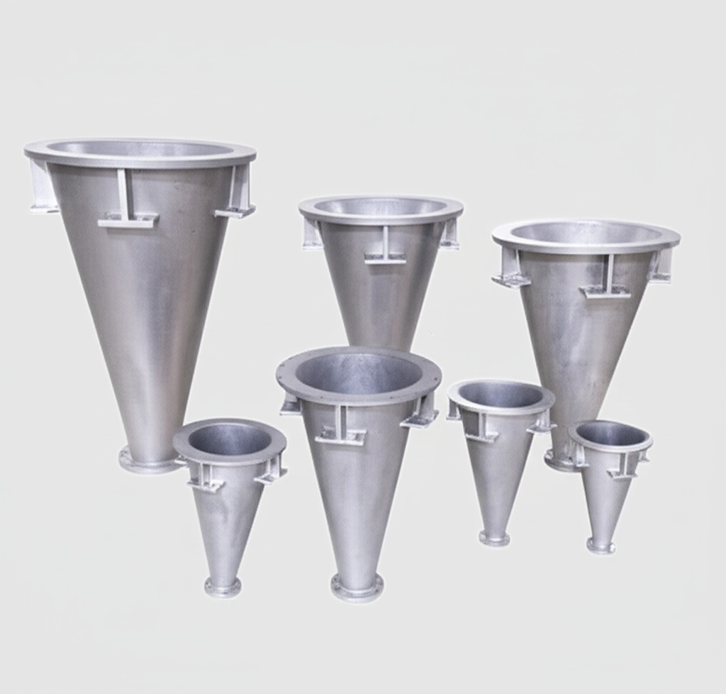
Advantages of Custom SiC Wafers for Specialized Requirements
While standard SiC wafers cater to a broad range of applications, many cutting-edge technologies demand custom SiC wafers tailored to specific performance targets. Bespoke SiC solutions offer several distinct advantages for OEMs and high-tech manufacturers:
- Optimized Performance: Customization allows for fine-tuning wafer parameters such as resistivity, thickness, orientation, and epitaxial layer specifications to precisely match the requirements of a particular device or application. This can lead to significant performance gains that are unachievable with off-the-shelf wafers.
- Specific Doping Profiles: For advanced power devices, precise control over doping concentrations (N-type or P-type) and profiles within the epitaxial layers is crucial. Custom wafer providers can offer highly specific doping to achieve desired electrical characteristics like threshold voltage and breakdown voltage.
- Unique Geometries and Sizes: While standard diameters (e.g., 100mm, 150mm, 200mm) are common, some applications may benefit from non-standard sizes or specific flats/notches. Customization can accommodate these unique geometrical needs.
- Tailored Surface Characteristics: Surface roughness, cleanliness, and passivation layers can be customized to ensure optimal compatibility with subsequent device fabrication processes, improving yield and reliability.
- Proprietary Epitaxial Structures: Companies developing novel device architectures often require proprietary multi-layer epitaxial structures. A flexible SiC wafer foundry can work collaboratively to develop and produce these custom epi-wafers.
- Enhanced Material Grades: For extremely demanding applications, such as those in aerospace or high-reliability defense systems, custom wafers can be produced using select, ultra-high-purity SiC boules with exceptionally low defect densities.
Engaging with a supplier specializing in customizing support for SiC wafers allows businesses to push the boundaries of their technology. This collaborative approach ensures that the foundational material itself is engineered for peak performance, giving a competitive edge in highly specialized markets. This is particularly relevant for industries like aerospace, defense, and advanced medical devices where off-the-shelf solutions may not suffice.
Navigating SiC Wafer Specifications: Diameter, Thickness, and Quality Grades
Procurement managers and engineers sourcing SiC wafers must navigate a range of critical specifications to ensure the material meets their application needs. Understanding these parameters is key to selecting the right product and supplier.
Key SiC Wafer Specifications:
- Diameter: Common SiC wafer diameters include 100mm (4-inch), 150mm (6-inch), and increasingly 200mm (8-inch). Larger diameters generally lead to lower per-die costs due to higher throughput in device fabrication.
- Polytype: The most common polytype for power electronics is 4H-SiC due to its superior electron mobility and higher breakdown field compared to other polytypes like 6H-SiC. 3C-SiC is also being explored for specific applications.
- Conductivity Type:
- N-type SiC: Doped with nitrogen, commonly used for MOSFETs and Schottky diodes. Resistivity is a key parameter.
- P-type SiC: Doped with aluminum, used in certain device structures.
- Semi-insulating (SI) SiC: High resistivity, often Vanadium-doped or intrinsically high purity, used as substrates for GaN-on-SiC RF devices.
- Resistivity: A measure of the material’s opposition to current flow. This is critical for defining the electrical characteristics of the final device (e.g., breakdown voltage, on-resistance). Ranges can vary widely based on doping levels.
- Thickness: Wafer thickness typically ranges from 350 µm to 500 µm, but custom thicknesses can be achieved. Thinner wafers can reduce on-resistance but require careful handling.
- Orientation: Typically, SiC wafers are offered with an off-axis cut (e.g., 4° off towards <11-20>) to facilitate high-quality epitaxial growth by reducing certain types of defects.
- Defect Density: This is a crucial quality metric. Key defects include:
- Micropipe Density (MPD): Zero MPD is often required for high-voltage devices.
- Basal Plane Dislocation (BPD) Density: Affects device reliability and performance.
- Threading Screw Dislocations (TSD) and Threading Edge Dislocations (TED): Impact device yield.
- Surface Roughness (Ra or Rms): A smooth, epi-ready surface is essential for high-quality epitaxial layer growth and subsequent device fabrication. Values are typically in the sub-nanometer range after Chemical Mechanical Polishing (CMP).
- Total Thickness Variation (TTV) and Bow/Warp: These geometrical parameters affect lithography and other processing steps. Tight control is necessary for high-yield manufacturing.
When specifying SiC wafers, it’s vital to discuss these parameters in detail with potential suppliers. A clear understanding of the application’s tolerance for each specification will guide the selection of the appropriate wafer grade and help in managing costs. Reputable suppliers will provide detailed datasheets and certificates of conformity.
The Manufacturing Journey: From Raw SiC to Precision Wafers
The production of high-quality SiC wafers is a complex, multi-step process that demands stringent control and advanced technology. Understanding this journey helps appreciate the value and cost associated with these advanced materials.
- SiC Powder Synthesis: The process begins with high-purity silicon and carbon sources, which are reacted at very high temperatures (e.g., Acheson process or Lely process for raw SiC powder) to form SiC grains.
- SiC Crystal Growth (Boule Formation): The most common method for growing single-crystal SiC boules for wafers is the Physical Vapor Transport (PVT) method, also known as the modified Lely method. High-purity SiC powder is sublimated at temperatures exceeding 2000°C in a controlled atmosphere. The SiC vapor then recrystallizes on a SiC seed crystal to form a large single crystal (boule). This step is critical for determining the polytype (e.g., 4H-SiC) and initial defect density.
- Boule Shaping and Orientation: The grown boule is then precisely machined to the desired diameter and a flat or notch is ground to indicate crystal orientation.
- Wafer Slicing: The oriented boule is sliced into thin wafers using advanced diamond wire saws. This step requires high precision to minimize kerf loss and maintain thickness uniformity.
- Lapping and Grinding: Sliced wafers undergo mechanical lapping and grinding processes to remove saw marks, achieve the target thickness, and improve surface flatness.
- Polishing: Wafers are polished using progressively finer diamond slurries to achieve a mirror-like surface. The final step is typically Chemical Mechanical Polishing (CMP), which produces an atomically smooth, damage-free “epi-ready” surface with extremely low roughness (typically <0.5 nm Ra).
- Cleaning and Inspection: Wafers are subjected to rigorous cleaning processes to remove any contaminants. They are then inspected for various parameters, including surface defects, resistivity, thickness, TTV, bow, warp, and crystallographic defects using sophisticated metrology tools.
- Epitaxial Growth (Optional but common for device wafers): For most power device applications, one or more thin layers of SiC with specific doping and thickness (epitaxial layers or “epi-layers”) are grown on the substrate wafer. This is typically done via Chemical Vapor Deposition (CVD). The quality of the SiC epitaxy is paramount for device performance.
Each step in this manufacturing journey is capital-intensive and requires specialized expertise. The challenges associated with growing large, low-defect SiC crystals and processing them into high-quality wafers contribute to the higher cost of SiC compared to silicon. However, the performance benefits often justify this investment for demanding power electronic applications.
Overcoming Challenges in SiC Wafer Production and Adoption
Despite the significant advantages of silicon carbide, its widespread adoption, particularly in cost-sensitive B2B markets, faces several challenges related to production and implementation. Understanding and mitigating these hurdles is key for both SiC wafer suppliers and end-users.
Key Challenges:
- High Material Cost: The intrinsic difficulties in growing high-quality SiC crystals (high temperatures, slow growth rates) and the complex wafering process contribute to SiC wafer costs being significantly higher than traditional silicon wafers.
- Mitigation: Continuous R&D in crystal growth (e.g., larger diameter boules), improved slicing techniques, and higher manufacturing yields are gradually reducing costs. Economies of scale as demand increases also play a crucial role. For buyers, strategic sourcing and long-term partnerships can help manage costs.
- Defect Control: Defects such as micropipes, basal plane dislocations (BPDs), stacking faults, and surface particulates can severely impact device performance and yield. Controlling these defects throughout the manufacturing process is a major challenge.
- Mitigation: Advanced crystal growth techniques, meticulous process control, improved polishing methods (like CMP), and stringent metrology are employed. Suppliers invest heavily in defect reduction R&D. Buyers should look for suppliers with robust quality control and defect characterization capabilities.
- Manufacturing Complexity and Yield: The hardness and chemical inertness of SiC make it difficult to machine, slice, and polish. This complexity can lead to lower yields compared to silicon processing.
- Mitigation: Development of specialized equipment (e.g., diamond wire saws, advanced CMP tools) and optimized process parameters are crucial. Experienced manufacturers with deep material science knowledge are better equipped to handle these complexities.
- Epitaxial Growth Uniformity: Achieving highly uniform thickness and doping concentration in SiC epitaxial layers, especially over large-area wafers, is challenging but critical for consistent device performance.
- Mitigation: Advanced CVD reactor designs, precise precursor flow control, and in-situ monitoring techniques help improve epi-layer uniformity.
- Device Fabrication Learning Curve: Fabricating reliable SiC devices requires specialized knowledge and processes different from silicon, including high-temperature ion implantation and annealing.
- Mitigation: Collaboration between wafer suppliers and device manufacturers, along with investment in SiC-specific fabrication lines and expertise, is essential. Some wafer suppliers also offer technology transfer and process integration support.
- Thermal Management at the System Level: While SiC devices can operate at higher temperatures, efficiently removing heat at the package and system level remains a design consideration to fully leverage SiC’s potential.
- Mitigation: Advanced packaging materials and thermal interface materials (TIMs) with high thermal conductivity, along with innovative cooling solutions, are being developed.
Overcoming these challenges requires a concerted effort from the entire SiC ecosystem, including material suppliers, equipment manufacturers, device fabricators, and system designers. For industrial buyers, partnering with knowledgeable and technologically advanced silicon carbide suppliers who are actively working on these issues is critical for successful SiC adoption.
Choosing Your SiC Wafer Supplier: Critical Factors for B2B Buyers
Selecting the right SiC wafer supplier is a critical decision for any company looking to integrate SiC technology into their products. For B2B buyers, procurement managers, and engineers, the evaluation process should go beyond just price. Here are key factors to consider:
- Material Quality and Consistency:
- Verify the supplier’s ability to consistently provide wafers with low defect densities (MPD, BPD, TSD), tight control over resistivity, thickness uniformity, and excellent surface finish.
- Request sample wafers for evaluation and ask for detailed Certificates of Conformance (CoC) with comprehensive metrology data for each shipment.
- Technical Expertise and Support:
- Assess the supplier’s R&D capabilities and their understanding of SiC material science and device physics.
- A supplier that can offer technical consultation, custom SiC wafer development, and support for process integration can be an invaluable partner.
- Manufacturing Capabilities and Capacity:
- Evaluate their crystal growth, slicing, polishing, and epitaxial growth facilities. Do they have the capacity to meet your volume requirements and scale with your demand?
- Inquire about their quality management systems (e.g., ISO 9001 certification) and process control methodologies.
- Customization Capabilities:
- If your application requires non-standard specifications (e.g., specific doping profiles, unique orientations, tailored epi-layers), ensure the supplier has proven experience in custom SiC wafer manufacturing.
- Supply Chain Reliability and Lead Times:
- Understand their typical lead times for various wafer types and their ability to manage supply chain disruptions.
- A reliable supply chain is crucial for uninterrupted production. Consider suppliers with robust inventory management and contingency plans.
- Cost-Effectiveness:
- While cost is a factor, it should be balanced against quality, reliability, and support. The cheapest option may not be the most cost-effective in the long run if it leads to lower device yields or performance issues.
- Seek transparent pricing and explore possibilities for volume discounts or long-term supply agreements.
- Reputation and References:
- Look for established suppliers with a good track record in the industry. Request customer references or case studies relevant to your application area.
- Location and Logistics:
- Consider the supplier’s location and its impact on shipping costs, communication, and support. For instance, understanding the capabilities within major SiC hubs can be advantageous.
A strategic partnership with a capable SiC wafer supplier can significantly impact the success of your power electronics projects. Thorough due diligence is essential to ensure you secure a reliable source of high-quality materials tailored to your needs.
The Weifang Advantage: China’s Silicon Carbide Innovation Hub and Sicarb Tech
When considering global silicon carbide suppliers, it’s impossible to overlook the significant advancements and manufacturing capabilities emerging from China. Specifically, Weifang City has established itself as the hub of China’s silicon carbide customizable parts manufacturing. This region is home to over 40 SiC production enterprises of various sizes, collectively accounting for more than 80% of the nation’s total SiC output.
Our strengths lie in:
- Deep Expertise: Sicarb Tech boasts a domestic top-tier professional team specializing in the customized production of silicon carbide products, including high-quality SiC wafers. We have supported over 32 local enterprises with our advanced technologies.
- Comprehensive Technological Capabilities: We possess a wide array of technologies spanning material science, process engineering, design, metrology, and evaluation, covering the integrated process from raw materials to finished SiC wafers and components. This enables us to meet diverse customization needs effectively.
- Quality and Cost-Competitiveness: We are committed to offering higher-quality, cost-competitive customized silicon carbide components and wafers from China, backed by reliable quality and supply assurance.
- Technology Transfer and Turnkey Solutions: Beyond supplying components, Sicarb Tech is also dedicated to global collaboration. If your organization is considering establishing a professional SiC products manufacturing plant in your country, we can provide comprehensive technology transfer for professional silicon carbide production. This includes a full range of turnkey project services such as factory design, procurement of specialized equipment, installation and commissioning, and trial production, ensuring a more effective investment and reliable technology transformation. Explore our tech transfer solutions.
Partnering with Sicarb Tech means accessing the heart of China’s SiC innovation ecosystem, benefiting from cutting-edge technology, experienced professionals, and a commitment to quality and customer success in the realm of custom SiC wafers and other SiC products.
Future Trends and Innovations in Silicon Carbide Wafer Technology
The field of silicon carbide wafer technology is dynamic, with ongoing research and development focused on pushing the boundaries of performance, cost, and applicability. Several key trends and innovations are shaping the future of SiC wafers for power electronics and other demanding applications:
- Larger Diameter Wafers: The industry is steadily moving towards larger wafer diameters, with 200mm (8-inch) SiC wafers becoming more prevalent. The development of 300mm (12-inch) SiC wafers is also underway. Larger wafers significantly reduce the per-die manufacturing cost, making SiC devices more economically viable for a wider range of applications, including high-volume markets like automotive.
- Improved Crystal Quality and Reduced Defects: Continuous advancements in PVT crystal growth and boule processing are leading to SiC substrates with even lower densities of critical defects like micropipes, BPDs, and TSDs. This directly translates to higher device yields, better performance, and enhanced reliability of SiC power devices.
- Thinner Wafers and Advanced Handling: Reducing wafer thickness can lower the on-resistance (RDS(on)) of vertical power devices, improving efficiency. Innovations in wafer grinding, polishing, and handling techniques for thin wafers are crucial for realizing these benefits without compromising mechanical integrity.
- Smart Cut / Layer Transfer Technologies: Techniques similar to Smart Cut™ (used in Silicon-on-Insulator manufacturing) are being explored for SiC. These methods could allow for the creation of thin, high-quality SiC layers on alternative, less expensive carrier

About the Author: Sicarb Tech
We provide clear and reliable insights into silicon carbide materials, component manufacturing, application technologies, and global market trends. Our content reflects industry expertise, practical experience, and a commitment to helping readers understand the evolving SiC landscape.

Customizable SiC
You May Also Interest
-
![]()
SiC Substrates: Key to Electronic Device Advances
SiC Substrates: Key to Electronic Device Advances Introduction: The Pivotal Role of SiC Substrates In the rapidly evolving landscape of high-performance industrial applications, materials science plays a crucial role. Among advanced materials, silicon carbide (SiC) stands out, particularly in the form of SiC substrates. These substrates are not merely foundational layers; they are critical enablers…
-
![]()
SiC Innovation via University Research Links
SiC Innovation via University Research Links In the rapidly evolving landscape of advanced materials, custom silicon carbide (SiC) stands out as a true game-changer. Its unparalleled properties make it indispensable across a spectrum of demanding industrial applications, from the cutting edge of semiconductor manufacturing to the extreme environments of aerospace and nuclear energy. But what…
-
![]()
SiC’s Potential Role in Quantum Computing Tech
SiC’s Potential Role in Quantum Computing Tech In the rapidly evolving landscape of advanced materials, silicon carbide (SiC) stands out as a material of exceptional promise. Traditionally lauded for its superior thermal, mechanical, and electrical properties, SiC is now garnering significant attention for its potential to revolutionize quantum computing. For engineers, procurement managers, and technical…