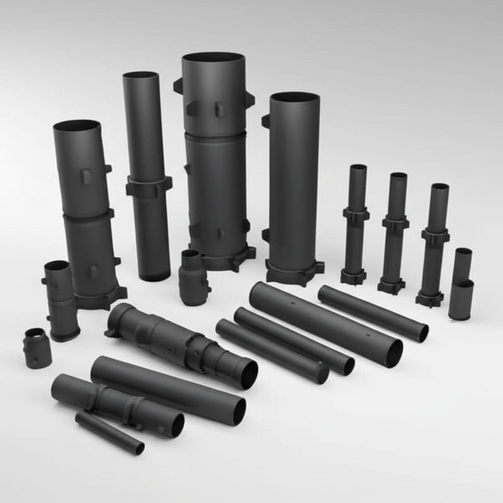
Microelectronics: The Power of SiC Inside
Share
Microelectronics: The Power of SiC Inside
Introduction: The Semiconductor Revolution with Custom Silicon Carbide
In the relentless pursuit of more efficient, powerful, and compact electronic systems, the microelectronics industry stands at the cusp of a significant transformation, largely driven by the advent of advanced materials. Among these, silicon carbide (SiC) has emerged as a frontrunner, promising to redefine the boundaries of performance in high-power and high-frequency applications. Custom silicon carbide products are not merely an incremental improvement; they represent a foundational shift, offering unparalleled thermal conductivity, higher breakdown electric field strength, and a wider bandgap compared to traditional silicon. These intrinsic properties make SiC an essential material for next-generation microelectronic devices, critical for industries ranging from automotive and aerospace to renewable energy and telecommunications. As demand for superior performance, energy efficiency, and operational reliability in extreme conditions grows, the role of custom SiC components—tailored to specific application needs—becomes increasingly vital. This blog post delves into the transformative power of silicon carbide in microelectronics, exploring its applications, advantages, design considerations, and the factors that make a reliable SiC supplier indispensable for manufacturers aiming to stay ahead in a competitive landscape. We will explore why engineers, procurement managers, and technical buyers are increasingly turning to specialized custom SiC solutions to unlock new possibilities in device performance and system efficiency.
The journey of silicon carbide from a niche material to a cornerstone of modern microelectronics is a testament to its exceptional characteristics. Its ability to operate at higher temperatures, voltages, and frequencies opens doors for innovation that were previously unattainable with silicon-based technologies. For businesses in semiconductor manufacturing, power electronics, and beyond, understanding and leveraging the capabilities of custom SiC is no longer optional but a strategic imperative for future growth and technological leadership.
The Expanding Role of SiC in Microelectronics: Diverse Applications
Silicon carbide’s unique electronic and thermal properties have propelled its adoption across a diverse array of microelectronic applications, fundamentally changing how power is managed, converted, and controlled. Its superior performance characteristics are particularly impactful in high-demand sectors.
- Power Electronics: SiC-based devices such as MOSFETs, Schottky diodes, and power modules are revolutionizing power conversion. They enable significantly higher switching frequencies and operating temperatures, leading to smaller, lighter, and more efficient power supplies, inverters, and converters. This is critical for electric vehicles (EVs), renewable energy systems (solar and wind inverters), and industrial motor drives. The demand for SiC power devices is rapidly increasing.
- Automotive Industry: Beyond EV powertrains (inverters, on-board chargers, DC-DC converters), SiC is finding use in various automotive sensors and high-temperature electronics, contributing to enhanced vehicle performance, range, and reliability.
- Aerospace and Defense: The ability of SiC to withstand harsh environments—high temperatures, radiation, and mechanical stress—makes it ideal for aerospace and defense applications. This includes power systems for satellites, radar systems, and avionics, where reliability and performance are paramount. High-temperature SiC electronics are crucial here.
- Renewable Energy: SiC inverters are key to improving the efficiency of solar and wind energy conversion, maximizing power output and reducing system costs. Their robustness also contributes to longer operational lifetimes in demanding outdoor conditions.
- Telecommunications: In 5G and future communication technologies, SiC is used in radio frequency (RF) power amplifiers and high-frequency devices, offering better performance and thermal management for base stations and other infrastructure components.
- Industrial Manufacturing: High-power SiC devices improve the efficiency of industrial equipment, including induction heating systems, welding power supplies, and uninterruptible power supplies (UPS), leading to energy savings and enhanced productivity. Industrial SiC components are becoming standard.
- LED Manufacturing: While GaN-on-SiC is common, SiC substrates themselves play a role due to their thermal properties, contributing to the longevity and performance of high-brightness LEDs.
- High-Temperature Sensors: SiC’s stability at extreme temperatures allows for the development of sensors capable of operating in environments where silicon-based sensors would fail, such as in combustion engines, turbines, and industrial process monitoring.
The integration of custom silicon carbide wafers and epitaxy is fundamental to these applications, allowing for the precise tailoring of material properties to meet the specific demands of each use case. As technology evolves, the applications for SiC in microelectronics are expected to expand even further, driving innovation and efficiency across numerous industries.
Why Custom SiC is Revolutionizing Microelectronics
The shift towards custom silicon carbide solutions in microelectronics isn’t just a trend; it’s a strategic response to the growing demand for higher performance, increased efficiency, and enhanced reliability in electronic devices and systems. Off-the-shelf components can offer general benefits, but custom SiC fabrication allows engineers to unlock the material’s full potential by tailoring its properties and design to specific, often demanding, application requirements.
Key advantages driving this revolution include:
- Optimized Thermal Management: SiC possesses a thermal conductivity approximately three times higher than silicon. Custom SiC components can be designed with specific geometries and integration features that maximize heat dissipation. This is crucial for high-power density applications, allowing devices to run cooler, reducing the need for bulky cooling systems, and extending operational life. For instance, custom heat spreaders or substrates can be tailored to the thermal profile of a specific power module.
-
Enhanced Electrical Performance:
- Higher Voltage Operation: SiC’s breakdown electric field is about ten times that of silicon. Customization allows for device structures (e.g., specific doping profiles, junction termination extensions in SiC MOSFETs) optimized for very high voltage ratings without compromising on-resistance or switching speed.
- Higher Switching Frequencies: SiC devices can switch much faster than silicon counterparts, leading to smaller passive components (inductors, capacitors) and thus more compact and lighter systems. Custom designs can fine-tune gate characteristics and reduce parasitic capacitances for optimal switching performance.
- Lower Energy Losses: The wider bandgap and lower on-resistance (RDS(on)) of SiC devices translate to significantly reduced conduction and switching losses. Customization can further minimize these losses by optimizing die size, active area, and internal structures for a particular operating point.
- Increased Power Density: The combination of superior thermal and electrical properties allows for a much higher power density. Custom SiC components enable the design of more powerful devices in smaller packages, a critical factor in applications like electric vehicles, portable power systems, and compact industrial drives.
- Improved Reliability in Harsh Environments: SiC’s inherent robustness means it can operate reliably at temperatures exceeding 200°C, and is more resistant to radiation. Customization can involve specific packaging solutions or material compositions that further enhance this resilience for aerospace, downhole drilling, or heavy industrial applications.
- Application-Specific Form Factors: Not all applications can accommodate standard component sizes or shapes. Custom SiC parts can be manufactured in unique geometries, thicknesses, and with specific metallization or interface layers to seamlessly integrate into complex or space-constrained systems. This includes custom-sized wafers, uniquely shaped substrates, or integrated sensor elements.
- Reduced System-Level Costs: While SiC material itself can be more expensive than silicon, custom SiC solutions often lead to lower overall system costs. This is achieved through increased efficiency (less energy wasted), reduced cooling requirements, smaller peripheral components, and longer system lifespan with less maintenance.
By opting for custom silicon carbide, companies can gain a significant competitive edge, developing products that are not only more efficient and reliable but also specifically optimized for their target market’s unique challenges. This tailored approach is what truly revolutionizes microelectronic design and performance.
Key SiC Material Grades for Microelectronic Applications
The exceptional performance of silicon carbide in microelectronics is rooted in its various polytypes, each possessing distinct crystal structures and electronic properties. The choice of SiC grade is critical and depends heavily on the specific application requirements. The most prominent polytypes for microelectronic devices are 4H-SiC and 6H-SiC, with Lely-grown and Van Arkel (CVD) SiC often referring to growth methods or specialized high-purity forms.
| SiC Polytype/Grade | Key Properties | Primary Microelectronic Applications | Considerations |
|---|---|---|---|
| 4H-SiC (Hexagonal) |
|
High-power, high-frequency devices:
Preferred for most modern power devices. |
Dominant choice for vertical power devices due to superior electron mobility. Can have higher basal plane dislocation (BPD) density, though advancements are mitigating this. Requires high-quality SiC epitaxy for optimal device performance. |
| 6H-SiC (Hexagonal) |
|
Historically used for:
Less common for new power device designs now. |
Lower electron mobility and higher anisotropy compared to 4H-SiC makes it less ideal for high-performance power switching. However, its technology is well-established for certain substrate applications. |
| 3C-SiC (Cubic) |
|
Research and niche applications:
|
Growth of high-quality, thick 3C-SiC layers on silicon is challenging due to lattice and thermal expansion mismatches, leading to high defect densities. Not yet widely adopted for mainstream power electronics. |
| High-Purity Semi-Insulating (HPSI) SiC |
|
Substrates for:
Requires excellent thermal conductivity and electrical insulation. |
Critical for RF applications to minimize substrate losses and ensure device isolation. Vanadium doping or intrinsic defect engineering is used to achieve semi-insulating properties. Quality of high-purity SiC substrates is paramount. |
Beyond these polytypes, the quality of the SiC material, particularly in wafer form, is paramount. This includes factors like:
- Micropipe Density (MPD): These are screw dislocation defects that can be device killers, especially in high-power applications. Modern SiC wafers aim for near zero micropipe density.
- Basal Plane Dislocation (BPD) Density: BPDs can propagate into the epitaxial layer and affect device performance and reliability, particularly for bipolar devices.
- Stacking Faults: These can increase the on-state voltage of PiN diodes and BJTs over time.
- Surface Quality and Flatness: Essential for subsequent epitaxial growth and photolithography processes.
Selecting the appropriate SiC grade and ensuring high material quality are foundational steps in manufacturing reliable and efficient microelectronic devices. For procurement managers and technical buyers, specifying the correct grade and understanding the implications of material defects are crucial when sourcing custom SiC wafers or substrates.
Critical Design Considerations for SiC-based Microelectronics
Designing microelectronic devices and systems with silicon carbide requires a nuanced approach that leverages its unique advantages while mitigating potential challenges. Engineers must consider several critical factors from the device level to the system integration to fully exploit SiC’s capabilities for high-power, high-temperature, and high-frequency applications.
-
Device Architecture Optimization:
- MOSFETs: Gate oxide reliability (SiO2/SiC interface) is a key concern. Interface trap density (Dit) affects channel mobility and threshold voltage stability. Passivation techniques, gate oxide materials, and annealing processes are critical. Design of the JFET region in trench MOSFETs or cell pitch in planar MOSFETs impacts RDS(on) and short-circuit withstand time.
- Diodes: For Schottky diodes, barrier height engineering is important for balancing forward voltage drop and reverse leakage current. Junction Barrier Schottky (JBS) and Merged PiN Schottky (MPS) designs enhance surge current capability and reduce leakage. For PiN diodes, managing bipolar degradation due to stacking fault expansion is crucial.
- Edge Termination: Due to SiC’s high breakdown field, effective edge termination structures (e.g., Junction Termination Extensions (JTE), field plates, guard rings) are essential to prevent premature breakdown at device peripheries and achieve theoretical blocking voltages. Customizing these structures for specific voltage classes is vital.
- Doping Profile Engineering: Precise control over doping concentrations (n-type and p-type) in drift layers, channel regions, and contact layers is fundamental. The high activation energies of some dopants in SiC necessitate high-temperature annealing. For custom SiC solutions, specific doping profiles can be requested to optimize device characteristics like breakdown voltage, on-resistance, and switching speed.
- Thermal Management Strategy: While SiC has excellent thermal conductivity, the high power densities achievable mean that thermal management at the die, package, and system level remains critical. Design considerations include die attach materials, substrate selection (e.g., direct bonded copper, active metal brazing), and heat sink design. Thermal modeling and simulation are essential.
- Gate Drive Design for SiC MOSFETs: SiC MOSFETs typically require specific gate drive voltages (e.g., +20V for turn-on, -2V to -5V for turn-off) to ensure low RDS(on) and prevent parasitic turn-on. Fast switching speeds necessitate gate drivers with high current sourcing/sinking capability and low parasitic inductance in the gate loop to minimize ringing and overshoot.
- Managing Parasitic Inductance and Capacitance: The fast dV/dt and dI/dt rates of SiC devices can exacerbate issues with parasitic inductance and capacitance in the package and PCB layout, leading to voltage overshoots, ringing, and EMI. Careful layout, minimizing loop areas, and using appropriate decoupling capacitors are crucial. Advanced packaging solutions for SiC power modules focus on minimizing these parasitics.
- Short-Circuit Protection: SiC MOSFETs generally have a lower short-circuit withstand time compared to silicon IGBTs due to their smaller die size for a given current rating. Robust and fast-acting short-circuit detection and protection mechanisms are vital.
- Material Quality and Defects: The design must account for the presence of material defects like BPDs and stacking faults, which can impact long-term reliability. Device designs may incorporate features to mitigate the impact of these defects, or stringent material specifications for SiC substrates are required.
- Cost vs. Performance Trade-offs: While SiC offers superior performance, it is generally more expensive than silicon. Designers must make informed decisions to balance the performance gains with the cost implications, considering the overall system benefits. Customization might involve optimizing die size for a specific current rating to manage cost effectively.
Addressing these design considerations effectively requires deep expertise in SiC device physics, fabrication processes, and application requirements. Collaboration with experienced technical ceramics suppliers and SiC specialists can provide valuable insights for optimizing designs.
Achieving Precision: Tolerance, Surface Finish & Wafer Quality in SiC Microelectronics
In the realm of silicon carbide microelectronics, precision is not just a goal; it’s a fundamental requirement for functionality and reliability. The manufacturing of SiC wafers, substrates, and custom components demands exceptionally tight control over dimensional tolerances, surface finish, and overall material quality. These factors directly impact downstream processes like epitaxial growth, photolithography, device fabrication, and ultimately, the performance and yield of SiC-based devices.
Dimensional Tolerances:
- Wafer Diameter and Thickness: Standard SiC wafers come in diameters like 100mm, 150mm, and increasingly 200mm. Thickness tolerances are typically within a few micrometers (µm) for prime wafers. For custom SiC parts, specific thicknesses or diameter modifications might be required, demanding precise cutting and grinding capabilities.
- Flatness (TTV, Bow, Warp): Total Thickness Variation (TTV), bow, and warp are critical parameters, especially for photolithography, where a very flat surface is needed for accurate pattern transfer. TTV is often specified in the range of ≤ 5 µm for prime wafers.
- Edge Profile and Exclusion Zone: Precisely shaped wafer edges minimize chipping and particle generation. The edge exclusion zone (typically 1-3 mm), where devices are not fabricated, also needs to be well-defined.
- Orientation Flats/Notches: These are critical for automated wafer handling and aligning crystallographic orientation for consistent device performance. Tolerances on their dimensions and angles are tight.
Surface Finish and Quality:
- Surface Roughness (Ra, Rq, Rz): An atomically smooth surface is essential for high-quality epitaxial growth. Typical surface roughness (Ra) for epi-ready SiC wafers is in the angstrom range (e.g., < 0.5 nm or even < 0.2 nm). This is achieved through meticulous chemical-mechanical polishing (CMP).
- Subsurface Damage: Grinding, lapping, and polishing processes can introduce subsurface damage. This damaged layer must be completely removed by CMP to ensure optimal electrical properties of the epitaxial layers grown on top.
- Scratches, Pits, and Stains: The surface must be free of visual defects like scratches, pits, and stains, which can interfere with device fabrication and act as nucleation sites for further defects. Automated inspection systems are used to classify and count such defects.
- Particulate Contamination: Strict cleanroom protocols and advanced cleaning techniques are employed to minimize particulate contamination on the wafer surface. Particle specifications are usually defined by size and count per unit area.
Wafer Quality (Material Integrity):
- Crystallinity and Polytype Uniformity: Ensuring a consistent polytype (e.g., 4H-SiC) across the entire wafer and minimizing the presence of other polytypes or misoriented grains is crucial. X-ray diffraction (XRD) is used for verification.
- Defect Density:
- Micropipe Density (MPD): As mentioned, this should be as close to zero as possible (e.g., < 0.1 cm-2 for high-quality commercial wafers).
- Basal Plane Dislocation (BPD) Density: Target values are typically < 500 cm-2 or lower, depending on the application.
- Threading Screw Dislocations (TSD) and Threading Edge Dislocations (TED): These also impact device performance and are carefully controlled.
- Resistivity Uniformity: For conductive or semi-insulating substrates, the resistivity must be uniform across the wafer to ensure consistent device behavior. This is verified using techniques like eddy current mapping or capacitance-voltage (C-V) measurements for HPSI SiC.
Achieving these stringent specifications requires sophisticated manufacturing processes, advanced metrology tools, and rigorous quality control systems. For technical buyers and procurement managers, it’s essential to clearly define these parameters when ordering SiC wafers or custom components. Partnering with a supplier that demonstrates a strong capability in precision machining, polishing, and defect characterization is paramount for successful SiC microelectronic device fabrication. Learn more about our customizing support for achieving the precise specifications your application demands.
Essential Post-Processing for SiC Microelectronic Devices
Once the basic silicon carbide device structures (like MOSFETs or diodes) are fabricated on the wafer, several critical post-processing steps are necessary to transform these structures into functional, reliable, and packageable devices. These steps are tailored to the specific requirements of SiC and the intended application, often demanding specialized techniques and equipment.
-
Backside Processing:
- Backgrinding/Thinning: Wafers are often thinned from their initial thickness (e.g., 350-500 µm) down to 100-200 µm or even less for power devices. This reduces thermal resistance and on-state resistance (VF or RDS(on)). Precision grinding is essential to maintain wafer integrity and flatness.
- Backside Metallization: After thinning, a metal stack is deposited on the backside of the wafer to form the drain contact (for vertical MOSFETs) or cathode contact (for diodes). Common metallization schemes include Ti/Ni/Ag or Ti/Ni/Au, chosen for good ohmic contact, solderability, and thermal conductivity. Sintering or annealing often follows to improve adhesion and contact resistance.
-
Wafer Dicing/Singulation: Individual dies are separated from the wafer. Due to SiC’s hardness and brittleness, this is a challenging step.
- Blade Dicing: Diamond-impregnated blades are commonly used but can cause chipping or micro-cracks. Optimization of blade type, spindle speed, and cutting fluid is critical.
- Laser Dicing/Ablation: Laser dicing offers a non-contact method that can reduce mechanical stress and chipping. Stealth dicing (internal wafer modification followed by breaking) or ablation cutting are options.
- Plasma Dicing: A dry etching process that can provide chip-free dicing, especially for thin wafers or complex die shapes.
-
Die Attach: The singulated SiC dies are attached to a lead frame, substrate (e.g., Direct Bonded Copper – DBC, or Active Metal Brazed – AMB substrate for modules), or package base.
- Sintering: Silver (Ag) sintering is increasingly popular for SiC due to its high thermal conductivity, high melting point, and reliability under thermal cycling. This is crucial for managing the high heat flux from SiC devices.
- Soldering: Traditional solders (e.g., AuSn, SAC alloys) can be used, but their lower melting points and fatigue resistance compared to sintered silver might limit performance in high-temperature applications.
- Epoxy Die Attach: Conductive epoxies can be used for lower power applications or where electrical isolation is needed from the backside.
-
Wire Bonding/Interconnects: Electrical connections are made from the top-side pads on the SiC die (source and gate for MOSFETs, anode for diodes) to the package leads or substrate.
- Aluminum (Al) Wire Bonding: Thick Al wires (100-500 µm) are common for power devices due to their high current carrying capability. Ultrasonic wedge bonding is typically used.
- Copper (Cu) Wire Bonding: Offers better electrical and thermal conductivity and improved reliability, but is harder to process.
- Ribbon Bonding: Al or Cu ribbons can offer lower loop inductance and higher current capacity than round wires.
- Flip-Chip or Solder Bumps: For advanced packaging, especially for RF devices or high-density modules, flip-chip bonding can reduce parasitics.
-
Passivation and Encapsulation:
- Surface Passivation: Additional dielectric layers (e.g., polyimide, silicon nitride) may be applied over the device surface (excluding bond pads) for enhanced protection against moisture, contaminants, and electrical arcing, especially for high-voltage devices.
- Encapsulation/Molding: The assembled device is encapsulated in a molding compound (e.g., epoxy-based) to provide mechanical protection, environmental sealing, and electrical insulation. Transfer molding is common for discrete packages, while gel fills or potting might be used for modules. The choice of encapsulant must consider SiC’s high operating temperatures.
- Testing and Burn-in: Final electrical testing is performed to ensure devices meet specifications. Burn-in or High-Temperature Reverse Bias (HTRB) testing may be conducted to screen out early failures and ensure long-term reliability of SiC microelectronic devices.
Each of these post-processing steps must be carefully optimized for SiC materials to maintain their inherent advantages and ensure the final product’s quality and reliability. This specialized handling highlights the need for expertise in advanced ceramics manufacturing w

About the Author: Sicarb Tech
We provide clear and reliable insights into silicon carbide materials, component manufacturing, application technologies, and global market trends. Our content reflects industry expertise, practical experience, and a commitment to helping readers understand the evolving SiC landscape.

Customizable SiC
You May Also Interest
-
![]()
Key SiC Exporters in Asia for International Trade
Key SiC Exporters in Asia for International Trade In the rapidly evolving landscape of advanced materials, silicon carbide (SiC) stands out as a material of unparalleled performance. Its exceptional properties make it indispensable across a spectrum of demanding industrial applications. For businesses seeking reliable and high-quality silicon carbide products, understanding the key players and regions…
-
![]()
SiC Substrates: Key to Electronic Device Advances
SiC Substrates: Key to Electronic Device Advances Introduction: The Pivotal Role of SiC Substrates In the rapidly evolving landscape of high-performance industrial applications, materials science plays a crucial role. Among advanced materials, silicon carbide (SiC) stands out, particularly in the form of SiC substrates. These substrates are not merely foundational layers; they are critical enablers…
-
![]()
SiC Innovation via University Research Links
SiC Innovation via University Research Links In the rapidly evolving landscape of advanced materials, custom silicon carbide (SiC) stands out as a true game-changer. Its unparalleled properties make it indispensable across a spectrum of demanding industrial applications, from the cutting edge of semiconductor manufacturing to the extreme environments of aerospace and nuclear energy. But what…