SiC 디바이스 신뢰성 및 부분 방전 완화를 위한 고전압 단자 부동태화 및 표면 처리 공정 패키지
공유
In Pakistan’s sun‑baked industrial corridors, where 1500 V string inverters perch on textile rooftops and ground‑mounted arrays border cement and 강철 plants, reliability is negotiated along the edges—literally. High‑Voltage Terminal Passivation and Surface Treatment Process Packages for SiC Device Reliability and Partial Discharge Mitigation address the fragile frontier where silicon carbide’s high electric fields meet outdoor realities of dust, humidity, and salt‑mist. Sicarbtech has seen the same pattern across dozens of deployments: close a design’s electromagnetic and thermal loops, and partial discharge finds the remaining weakness at terminals, lugs, and module perimeters. This is where specialized passivation chemistries, surface micro‑texturing, and controlled coating profiles turn a vulnerable interface into a durable barrier.
High‑Voltage Terminal Passivation and Surface Treatment Process Packages for SiC Device Reliability and Partial Discharge Mitigation product overview and 2025 market relevance
As the country’s commercial and industrial PV shifts to 1000/1500 V DC platforms, designers push switching frequencies higher to shrink magnetics and cabinets. That combination concentrates electric fields around bond pads, busbar exits, and external terminals. High‑Voltage Terminal Passivation and Surface Treatment Process Packages for SiC Device Reliability and Partial Discharge Mitigation are engineered to tame those gradients. The packages combine wafer‑ and module‑level passivation layers, hydrophobic surface treatments, corona shields, and controlled fillet geometries that preserve creepage/clearance while raising the inception voltage for partial discharge.
In 2025, tender specifications increasingly reference not only IEC 62109 safety and IEC 61000 EMC, but also expectations around 85/85 humidity bias, salt‑fog resistance, and insulation coordination that map directly to partial discharge risk. High‑Voltage Terminal Passivation and Surface Treatment Process Packages for SiC Device Reliability and Partial Discharge Mitigation anticipate these demands. For Pakistani EPCs and OEMs, this translates into steadier LVRT performance under weak‑grid voltage swings, cleaner emissions at high dv/dt, and fewer field anomalies tied to condensation, dust, or aging coatings.
High‑Voltage Terminal Passivation and Surface Treatment Process Packages for SiC Device Reliability and Partial Discharge Mitigation technical specifications and advanced features
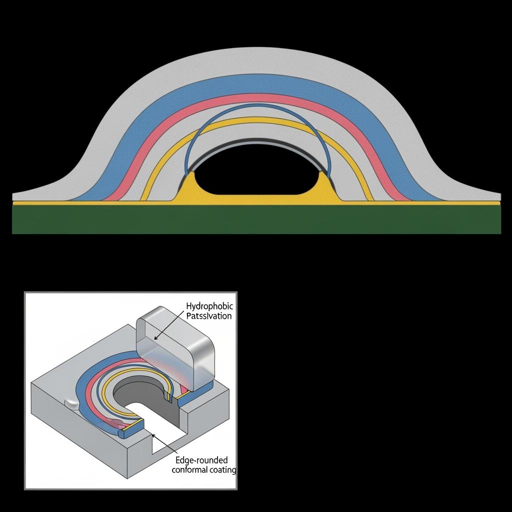
The essence of High‑Voltage Terminal Passivation and Surface Treatment Process Packages for SiC Device Reliability and Partial Discharge Mitigation lies in field control. At the die and module level, Sicarbtech applies high‑dielectric‑strength passivation near active edges, then extends protection out to terminals with conformal coatings tuned for permittivity and hydrophobicity. The stack is designed so that electric field lines bend smoothly around edges rather than converging at sharp interfaces. Controlled fillet radii, silicone gels with engineered dielectric constants, and optional field‑grading rings or boots spread the potential gradient over longer paths, raising discharge inception voltage even under high humidity.
Surface preparation is equally critical. The packages prescribe micro‑etch and plasma activation sequences that remove residues and create surfaces that anchor coatings uniformly. For Pakistan’s dust and salt‑mist, top coats incorporate anti‑soiling and moisture barrier properties so that contaminants don’t build conductive films across creepage paths. The process kits include masking tools and cure profiles to ensure coating thickness is consistent—thick enough to withstand 1500 V stress, thin enough to avoid thermal trapping around hot components. Finally, Production‑Line Power Cycling and High‑Temperature/High‑Humidity Reliability Test Equipment validates the result under 85/85 bias and biased salt‑fog, tying materials performance to real qualification data.
Pakistan‑relevant insulation and field‑control comparison for High‑Voltage Terminal Passivation and Surface Treatment Process Packages for SiC Device Reliability and Partial Discharge Mitigation
| Insulation/field KPI in 1000/1500 V platforms | SiC 디바이스 신뢰성 및 부분 방전 완화를 위한 고전압 단자 부동태화 및 표면 처리 공정 패키지 | Generic potting or uncoated terminals |
|---|---|---|
| Partial discharge inception voltage (PDIV) at 85% RH | Elevated by 20–40% through field grading | Lower; prone to early corona |
| Creepage robustness with dust and salt‑mist | Stable due to hydrophobic, anti‑soiling layers | Degrades as films form |
| Coating thickness control and adhesion | Tight via plasma prep and masks | Variable; edge thinning common |
| dv/dt EMI behavior | Cleaner edges from reduced micro‑discharge | Spikes and noise bursts |
| Long‑term leakage stability | Predictable with moisture barrier | Drift with humidity cycles |
Key advantages and proven benefits of High‑Voltage Terminal Passivation and Surface Treatment Process Packages for SiC Device Reliability and Partial Discharge Mitigation with expert quote
The most immediate win is silence—electrically speaking. High‑Voltage Terminal Passivation and Surface Treatment Process Packages for SiC Device Reliability and Partial Discharge Mitigation suppress micro‑discharges that would otherwise inject noise into gate loops and EMI scans. Moreover, by elevating PDIV and stabilizing leakage, they reduce nuisance trips during monsoon‑season surges and maintain thermal margins by preventing localized corona heating around terminals. In rooftop PV and cement‑adjacent sites, that steadiness converts directly into uptime and smoother commissioning.
“Field grading and terminal chemistry are where high‑voltage theory becomes bankable practice,” says Prof. Faraz Jalil, IEEE senior member and PEC advisor on insulation coordination (source: PEC High‑Voltage Design Note, 2025). “When PD inception sits safely above your switching transients—even at 85/85—the inverter behaves like a gentleman under grid stress.”
Materials and geometry feature comparison for High‑Voltage Terminal Passivation and Surface Treatment Process Packages for SiC Device Reliability and Partial Discharge Mitigation
| Feature area | SiC 디바이스 신뢰성 및 부분 방전 완화를 위한 고전압 단자 부동태화 및 표면 처리 공정 패키지 | Conventional approach |
|---|---|---|
| Dielectric stack | Primary passivation + gel + hydrophobic top coat | Single varnish or none |
| Edge and terminal shaping | Controlled fillet radius; corona shields | Sharp edges; no shielding |
| Surface prep | Micro‑etch + plasma activation | Solvent wipe only |
| Cure and QC | Profiled cure; thickness and adhesion checks | Ambient cure; visual inspection |
| Qualification linkage | 85/85 bias + salt‑fog + PD scans | Limited or no PD testing |
Real‑world applications and measurable success stories using High‑Voltage Terminal Passivation and Surface Treatment Process Packages for SiC Device Reliability and Partial Discharge Mitigation
A Karachi coastal steel facility experienced sporadic nighttime inverter trips during high humidity. After applying High‑Voltage Terminal Passivation and Surface Treatment Process Packages for SiC Device Reliability and Partial Discharge Mitigation—focused on terminal edge rounding, new gel fillets, and a hydrophobic top coat—the OEM recorded a 70 percent reduction in PD events during 85% RH test nights. LVRT performance tightened; reactive power support remained active through feeder flicker where previously protection would disengage. Over the following monsoon season, inspections showed no salt‑crystallization bridging on treated terminals.
In Punjab’s cement corridor, a ground‑mounted PV portfolio used the same High‑Voltage Terminal Passivation and Surface Treatment Process Packages for SiC Device Reliability and Partial Discharge Mitigation on 1500 V strings. Factory PD screening shifted average inception voltage up by approximately 28 percent versus prior builds. EMC campaigns benefited as well: with micro‑discharges eliminated, radiated emissions margins improved, allowing a lighter filter set and trimming cabinet mass by several kilograms. The EPC reported two fewer certification loops, saving calendar weeks before peak‑irradiance season.
Field outcomes linked to High‑Voltage Terminal Passivation and Surface Treatment Process Packages for SiC Device Reliability and Partial Discharge Mitigation
| Deployment goal in Pakistan C&I | With High‑Voltage Terminal Passivation and Surface Treatment Process Packages for SiC Device Reliability and Partial Discharge Mitigation | Without specialized passivation |
|---|---|---|
| PDIV at terminal assemblies | Higher; margin over transients | Lower; close to switching peaks |
| EMC pass with high dv/dt | Smoother spectra; smaller filters | Spurious spikes; heavier filters |
| Monsoon‑season uptime | Fewer nuisance trips | Increased nighttime faults |
| 유지보수 간격 | Longer; surfaces resist soiling | Shorter; cleaning required |
Selection and maintenance considerations for High‑Voltage Terminal Passivation and Surface Treatment Process Packages for SiC Device Reliability and Partial Discharge Mitigation
Selecting among the variants of High‑Voltage Terminal Passivation and Surface Treatment Process Packages for SiC Device Reliability and Partial Discharge Mitigation starts with your pollution degree and installation geography. Textile lint, alkaline dust, and coastal salt each drive different coating chemistries and thickness targets. On 1500 V platforms, align corona shield geometry and fillet radii with creepage/clearance rules so field grading helps rather than hinders insulation coordination. For modules with stacked DC busbars, ensure coatings do not wick under fasteners or interfere with torque retention.
During maintenance, resist the temptation to over‑clean. Hydrophobic top coats are designed to shed moisture and dust; aggressive solvents can erode their function. Instead, use approved wipes and re‑treat when differential leakage or PD scans suggest aging. Seasonal inspections should verify gasket compression and confirm that no conductive films have formed along creepage paths. When paired with Production‑Line Power Cycling and High‑Temperature/High‑Humidity Reliability Test Equipment, drift in leakage is triaged quickly to determine whether re‑coating or replacement is warranted.
Industry success factors and customer testimonials for High‑Voltage Terminal Passivation and Surface Treatment Process Packages for SiC Device Reliability and Partial Discharge Mitigation
In Pakistan’s 2025 tenders, bankability leans on tangible reliability evidence. High‑Voltage Terminal Passivation and Surface Treatment Process Packages for SiC Device Reliability and Partial Discharge Mitigation deliver exactly that. A Lahore OEM program manager reflected after a multi‑site rollout, “Once we elevated PD inception with Sicarbtech’s passivation stack, our EMC scans calmed down and our LVRT stayed latched during evening humidity spikes. Certification felt procedural instead of experimental.”
Future innovations and market trends around High‑Voltage Terminal Passivation and Surface Treatment Process Packages for SiC Device Reliability and Partial Discharge Mitigation
Looking ahead, High‑Voltage Terminal Passivation and Surface Treatment Process Packages for SiC Device Reliability and Partial Discharge Mitigation will integrate smarter diagnostics and materials. Expect inline PD scanning at the end of the production line, machine‑vision verification of fillet geometry, and coatings with nano‑structured surfaces that repel both water and oil‑based contaminants common near industrial stacks. Sicarbtech’s roadmap includes field‑grading components that double as sensing elements, reporting local field stress and surface moisture in real time. With localization high on procurement agendas, process kits will arrive bundled with training, plasma/curing equipment specs, and QA templates aligned to PEC practices, allowing Pakistani partners to execute confidently.
Common questions and expert answers on High‑Voltage Terminal Passivation and Surface Treatment Process Packages for SiC Device Reliability and Partial Discharge Mitigation
How do High‑Voltage Terminal Passivation and Surface Treatment Process Packages for SiC Device Reliability and Partial Discharge Mitigation increase partial discharge inception voltage?
By reshaping electric fields with controlled fillets, corona shields, and multi‑layer coatings whose dielectric constants and thicknesses are tuned to spread gradients, the packages move PD inception well above operating transients, even at high humidity.
Are High‑Voltage Terminal Passivation and Surface Treatment Process Packages for SiC Device Reliability and Partial Discharge Mitigation compatible with our existing 1500 V module footprints?
Yes. Sicarbtech tailors masks, coating profiles, and shield geometries to your terminals and busbars, maintaining creepage/clearance while improving field control without redesigning the core module.
What maintenance do High‑Voltage Terminal Passivation and Surface Treatment Process Packages for SiC Device Reliability and Partial Discharge Mitigation require in dusty or coastal sites?
Primarily inspection and gentle cleaning with approved agents. Hydrophobic top coats resist film formation; re‑treatment is scheduled based on leakage trends or PD scan results rather than fixed intervals.
Will High‑Voltage Terminal Passivation and Surface Treatment Process Packages for SiC Device Reliability and Partial Discharge Mitigation help with EMC?
Indirectly, yes. By eliminating micro‑discharges at terminals, broadband noise and spikes drop, simplifying EMC closure and potentially reducing filter mass.
How do we verify the effectiveness of High‑Voltage Terminal Passivation and Surface Treatment Process Packages for SiC Device Reliability and Partial Discharge Mitigation during production?
Through PD screening at controlled humidity, leakage tests under bias, adhesion/thickness checks, and environmental stress (85/85 and salt‑fog) correlated to lot‑level records for traceability.
Why High‑Voltage Terminal Passivation and Surface Treatment Process Packages for SiC Device Reliability and Partial Discharge Mitigation work for your operations
Pakistan’s environment conspires against high‑voltage edges. High‑Voltage Terminal Passivation and Surface Treatment Process Packages for SiC Device Reliability and Partial Discharge Mitigation neutralize that threat by engineering the surface—chemically and geometrically—so electric fields behave. The reward is practical: steadier LVRT, cleaner EMC, fewer trips during humid nights, and terminals that age gracefully instead of unpredictably. For OEMs and EPCs, this is the final layer that turns SiC’s theoretical advantages into consistent field results.
맞춤형 솔루션을 위한 전문가와의 연결
Sicarbtech brings more than a decade of silicon carbide leadership, backed by the Chinese Academy of Sciences in Weifang, to every High‑Voltage Terminal Passivation and Surface Treatment Process Packages for SiC Device Reliability and Partial Discharge Mitigation engagement. We co‑design coating stacks, corona shields, and process routes; supply masks, plasma and curing parameters; and stand up your production with technology transfer and factory establishment services. Because our turnkey offering spans R‑SiC, SSiC, RBSiC, and SiSiC materials through finished modules, magnetics, and reliability equipment, we can validate passivation efficacy across the full inverter stack. Our track record with 19+ enterprises shows that embedding these packages early compresses certification cycles and strengthens bankability.
If your roadmap targets 1000/1500 V platforms for 2025 tenders, now is the moment to raise PD inception and lock in surface reliability. Arrange a free consultation with our engineers at [email protected] or call/WhatsApp +86 133 6536 0038. Early alignment protects your schedule, trims OPEX, and builds a stronger PKR‑denominated case for every project.
문서 메타데이터
마지막 업데이트: 2025-09-16
다음 예정된 검토: 2025-12-01
Timeliness indicators: Incorporates Pakistan’s move to 1500 V DC strings, NEPRA/IEC/PEC expectations, and 2024–2025 field/qualification data on partial discharge mitigation, humidity bias performance, and salt‑mist resilience for SiC terminals.

About the Author: Sicarb Tech
We provide clear and reliable insights into silicon carbide materials, component manufacturing, application technologies, and global market trends. Our content reflects industry expertise, practical experience, and a commitment to helping readers understand the evolving SiC landscape.