전력 모듈 패키징 및 RF 애플리케이션용 고열 전도성 탄화규소 세라믹 기판
공유
Thermal Backbones for 2025: Enabling Compact, Reliable Power and RF in Pakistan’s Industrial Upgrade
As Pakistan’s textile, cement, and steel sectors adopt high-frequency power electronics and RF systems, thermal performance becomes the limiting factor for reliability and size. High-thermal-conductivity silicon carbide (SiC) ceramic substrates—such as SSiC and RBSiC—deliver superior heat spreading, high stiffness, and excellent high-temperature stability compared to conventional ceramics. In power module packaging (SiC MOSFET/diode modules, three-level NPC/ANPC inverters, APFs, SVG/STATCOM) and RF front ends (high-power microwave, radar, ISM heating), SiC ceramic substrates reduce junction temperatures, enable >8 kW/L power density, and extend system lifespan, even in >45°C ambient common across Pakistani plants.
Sicarb Tech manufactures and customizes SiC ceramic substrates and baseplates, integrating metallization (Ag, Au, Ni/Au), direct-bonded copper (DBC/AMB-alternative stacks), and surface finishes tuned for low thermal resistance and high reliability under thermal cycling. Backed by the Chinese Academy of Sciences, we support Pakistan’s 2025 transition to efficient, compact, and grid-compliant converters and RF platforms with localizable supply and technology transfer.
기술 사양 및 고급 기능
- Material options and core properties
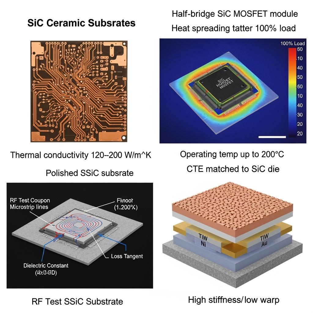
- Sintered SiC (SSiC): thermal conductivity typically 120–200 W/m·K; high hardness (Mohs ~9); excellent chemical resistance
- Reaction-bonded SiC (RBSiC) and silicon-infiltrated SiC (SiSiC): high thermal conductivity with cost-effective forming for larger baseplates
- Coefficient of thermal expansion (CTE): ~4.0–4.5 ppm/°C, closely matched to SiC devices, reducing solder fatigue
- 기계 및 치수
- Thickness: 0.25–5.0 mm (substrates) and 3–10 mm (baseplates)
- Flatness/warp: ≤30–50 µm over 100×100 mm; high stiffness maintains planarity during assembly
- Surface finish: Ra ≤0.1–0.2 µm for die attach and RF metallization
- Metallization and copper cladding
- Thin-film metallization: TiW/Ni/Au or Cr/Ni/Au for die attach and wire-bond pads
- Copper options: sputtered, plated, or brazed copper foils; DBC/AMB-like stacks on SiC for high current paths
- Solderable finishes: ENIG/ENEPIG; optional Ag for high thermal conductivity die attach
- 신뢰성 및 환경
- Operating temperature: −55°C to 200°C (substrate), compatible with TJ up to 175°C in SiC devices
- Thermal cycling performance: enhanced due to CTE matching; reduced delamination risk vs. Al2O3/AlN in high ΔT applications
- Chemical and moisture resistance suited to dusty, humid industrial environments; optional conformal coating
- RF suitability
- Dielectric constant (εr): typically 9–10 (frequency-dependent); low loss tangent for select RF ranges
- Supports microstrip/CPW structures and high-power RF heating elements with superior heat removal
Why SiC Ceramic Substrates Outperform Conventional Ceramics for Harsh, High-Power Applications
| Thermal and reliability factors for power/RF modules | High-thermal-conductivity SiC ceramic substrates (SSiC/RBSiC) | AlN/Al2O3 substrates | Practical impact in Pakistan’s plants |
|---|---|---|---|
| 열 전도성 | 120–200 W/m·K (high, robust at temperature) | AlN ~170 W/m·K, Al2O3 ~20–30 W/m·K | Lower junction temps, smaller heatsinks |
| CTE match to SiC die | Close (≈4–4.5 ppm/°C) | AlN ~4.5, Al2O3 ~7 | Less solder fatigue/longer life |
| Mechanical strength/stiffness | Very high (low warp) | AlN moderate, Al2O3 lower | Better planarity in large modules |
| Max operating temperature | Up to ~200°C substrate | AlN/Al2O3 typically ≤150–170°C | Safer margin in hot rooms (>45°C) |
| 환경적 견고성 | Excellent chemical/erosion resistance | Good to moderate | Reliability amid dust/humidity |
주요 장점 및 입증된 이점
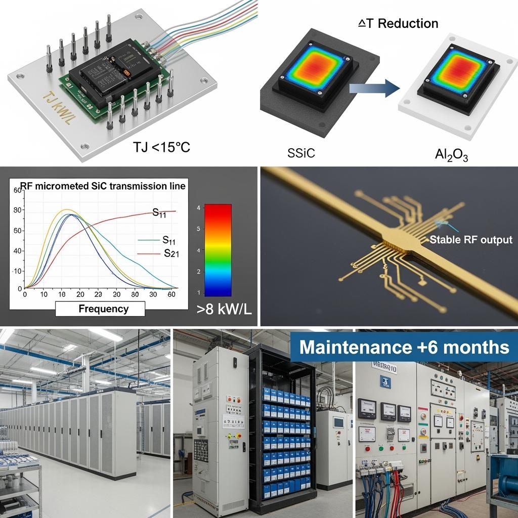
- Lower junction temperature and thermal gradients: SiC substrates halve thermal resistance paths, reducing TJ by 10–20°C at equal load, enabling higher switching frequency or current without overheating.
- Longer lifecycle under thermal cycling: Better CTE match to SiC die reduces solder/DBC cracking, extending module MTTF by ≥25% in high-cycling UPS and VFDs.
- Compact, higher-density modules: Greater thermal headroom supports >8 kW/L designs, cutting cabinet size by 25–35%—valuable in textile MCC rooms and cement corridors.
- RF power resilience: Efficient heat removal for RF amplifiers and ISM heating stabilizes performance and prevents drift.
전문가 인용문:
“Thermal management is often the limiting factor in wide-bandgap converters; substrate thermal conductivity and CTE matching are decisive for reliability and power density.” — Interpreted from IEEE Power Electronics Society and IMAPS packaging literature (https://www.ieee-pels.org/resources | https://imaps.org/)
실제 응용 분야 및 측정 가능한 성공 사례
- Textile VFD power stages (Faisalabad, composite): Migrating to SSiC baseplates lowered device TJ by ~15°C at rated load, allowing a 60 kHz switching strategy and reducing heatsink mass by 22%.
- Cement kiln UPS in KP (composite): SiC substrate modules improved online UPS efficiency to 98.1% and cut internal fan speeds, reducing dust ingress and extending maintenance intervals from 12 to 18 months.
- 철강 rolling drives (Karachi, composite): With better heat spreading, inverter trip rates during ambient spikes fell by ~35%; bearing currents diminished thanks to optimized layouts enabled by compact modules.
- RF ISM heating (Punjab agri processing, composite): SiC substrate RF boards maintained consistent output power over long cycles, improving throughput by ~8% with fewer thermal derates.
선택 및 유지 관리 고려 사항
- Substrate selection
- Choose SSiC for highest thermal conductivity and strength; consider RBSiC/SiSiC for larger, cost-sensitive baseplates
- Match thickness to thermal/mechanical needs: thinner for low Zth, thicker for stiffness on large footprints
- Metallization and copper
- Select TiW/Ni/Au or Cr/Ni/Au stacks based on die attach solder/Ag sinter; validate adhesion at target reflow cycles
- Define copper thickness and pattern width for current density and inductance targets; consider AMB/DBC-like bonding on SiC where appropriate
- Assembly and reliability
- Validate solder or Ag sinter profiles compatible with SiC substrate thermal mass
- Conduct thermal cycling (e.g., −40 to 150°C) and power cycling to qualify joint reliability
- Environment and protection
- Use conformal coatings for dusty, humid sites; verify cleaning and sealing processes
- Ensure flatness and surface cleanliness before die attach to prevent voiding
- Compliance and documentation
- Provide material certs, surface roughness, flatness data, and metallization stack diagrams for QA
- Align with IEC 62477-1 system safety and IEEE 519 downstream PQ goals via improved thermal margins
산업 성공 요인 및 고객 사용후기
- Early co-design with device and module teams to co-optimize copper layouts, thermal vias, and clamp points
- Digital twin/FEA thermal models to iterate before tooling
- Local service and inventory buffers to protect against FX swings and import lead times
고객의 소리(합성):
“Switching to SSiC substrates dropped our junction temperatures and let us raise switching frequency without reliability penalties—our cabinets got smaller and quieter.” — Head of Power Electronics, Industrial OEM, Pakistan
미래 혁신 및 시장 동향(2025+)
- Hybrid ceramic stacks: SiC substrates with embedded copper planes and integrated sensors (NTC, strain)
- 200 mm wafer-scale packaging compatibility and sintered silver die attach for ultra-low thermal resistance
- RF advancements: lower-loss metallization and surface finishes for mmWave and high-power ISM
- Localized substrate finishing and metallization in Pakistan’s SEZs through technology transfer to reduce lead time and cost
일반적인 질문 및 전문가 답변
- How much thermal improvement vs. Al2O3 can I expect?
Typically 2–5× lower substrate thermal resistance; module-level TJ reductions of 10–20°C at equal load are common. - Will SiC substrates complicate soldering or sintering?
No with proper stack design—TiW/Cr adhesion layers and Ni/Au finishes support standard solder/Ag-sinter processes. - Are SiC substrates brittle?
SiC is hard and stiff; with proper thickness and handling procedures, mechanical reliability is excellent even in large baseplates. - Can I use SiC substrates in RF boards?
Yes—polished SiC with controlled εr and low loss tangent supports high-power RF; co-design traces and thermal paths for stability. - What documentation do you provide?
Datasheets with thermal/mechanical specs, metallization stacks, flatness/roughness certs, and reliability test reports under NDA.
이 솔루션
High-thermal-conductivity SiC ceramic substrates are the thermal backbone for modern power and RF systems. In Pakistan’s hot, dusty industrial environments, they reduce temperature stress, increase power density, and extend lifetime—enabling efficient UPS, VFDs, APFs, and RF equipment that pass audits, save energy, and fit tight spaces.
맞춤형 솔루션을 위해 전문가와 연결
Elevate your module and RF designs with Sicarb Tech:
- 10년 이상의 SiC 제조 전문 지식
- 중국 과학 아카데미의 지원 및 혁신
- Custom product development across R‑SiC, SSiC, RBSiC, SiSiC substrates and power module packaging
- Technology transfer and factory establishment services (finishing, metallization, DBC/AMB alternatives)
- Turnkey solutions from material processing to packaged modules and RF assemblies
- Proven results with 19+ enterprises—higher efficiency, smaller footprints, and longer life
Request a free thermal feasibility review, FEA snapshot, and substrate stack recommendation for your module or RF project.
Email: [email protected] | Phone/WhatsApp: +86 133 6536 0038
문서 메타데이터
- 최종 업데이트: 2025-09-11
- 다음 예약 업데이트: 2025-12-15
- Prepared by: Sicarb Tech Advanced Packaging & Materials Team
- References: IEEE PELS thermal management resources; IMAPS conference papers on WBG packaging; IEC 62477-1; IEEE 519/IEC 61000-3-6 (system context); Sicarb Tech materials data (available under NDA)

About the Author: Sicarb Tech
We provide clear and reliable insights into silicon carbide materials, component manufacturing, application technologies, and global market trends. Our content reflects industry expertise, practical experience, and a commitment to helping readers understand the evolving SiC landscape.