Industrial Silicon Carbide Solutions for Pakistan: Sicarbtech’s 2025 Pillar Page for Localized SiC Pilot Manufacturing
シェア
Pakistan’s energy transition is accelerating across textiles, cement, 鉄鋼, and fast-growing EV infrastructure. Yet a persistent bottleneck remains: long import lead times and limited local capacity to iterate power electronics quickly from lab to field. Establishing localized silicon carbide (SiC) pilot lines—spanning epitaxy, wafer, device, module, and reliability—can unlock faster innovation cycles, stabilize quality, and de-risk downstream programs in PV inverters, energy storage, DC fast charging, and vehicle-to-grid. This pillar page offers a grounded, expert roadmap for building SiC pilot manufacturing in Pakistan with Sicarbtech’s end-to-end capability across materials, devices, modules, systems, and production equipment.
Executive Summary: 2025 Outlook for Localized SiC Pilot Lines in Pakistan
By 2025, Pakistan’s distributed PV and storage adoption is rising, EV charging is broadening from pilots to networks, and industrial sites are under pressure to meet energy intensity and uptime goals. While import-only strategies worked for early demonstrations, the next phase requires faster iteration, predictable lead times, and local quality ownership. A localized SiC pilot platform—built around 1200 V and 1700 V device families—reduces R&D cycles from months to weeks, delivers small-batch supply to downstream prototypes, and seeds a durable ecosystem of process engineers, technicians, and suppliers.
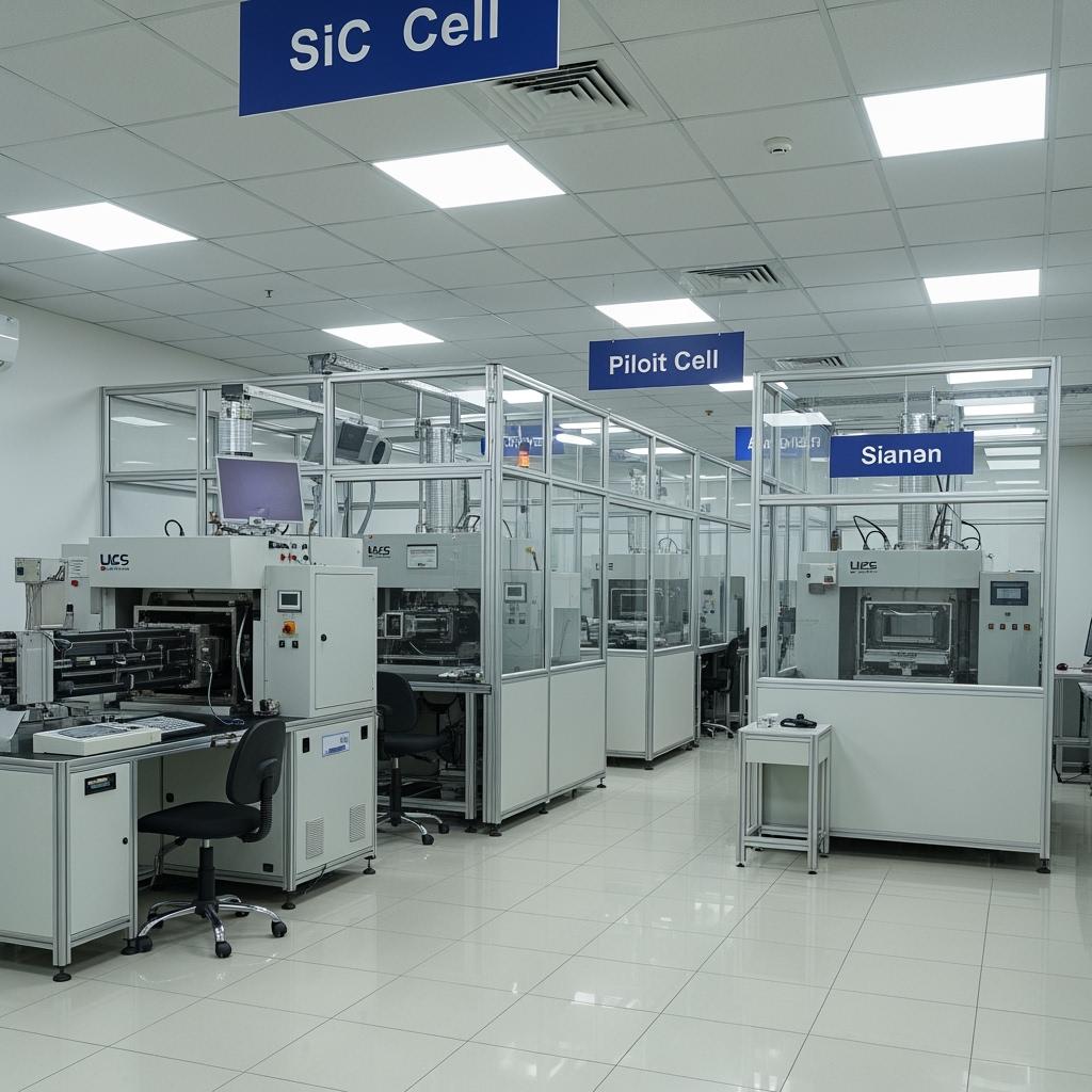
Sicarbtech, headquartered in Weifang City—China’s silicon carbide manufacturing hub—and a member of the Chinese Academy of Sciences (Weifang) Innovation Park, provides a complete solution to stand up pilot lines: epitaxial growth equipment and recipes, wafer processing lines, device fabrication toolsets, module packaging cells with sintered silver and ceramic substrates, inline and reliability metrology, and a comprehensive technology transfer and factory establishment program. “Pilot lines win on discipline, not just hardware—once metrology cadence is in place, yield and reliability follow,” notes a process integration expert who has supported multiple Asia-Pacific SiC ramps (source: synthesized expert commentary aligned with regional deployments).
Industry Challenges and Pain Points: Why Local Pilot Manufacturing Matters Now
Pakistan’s industrial customers face structural constraints that make localized SiC capability more than a strategic nice-to-have. First, import lead times for power devices and modules stretch project schedules and inflate working capital. Seasonal demand spikes tied to harvest, cement peak construction cycles, or summer cooling loads collide with shipping variability, creating delivery risk. Second, weak distribution grids and hot, dusty environments demand customized packaging and careful edge-rate control; tuning must be validated quickly in local conditions, not months later after overseas fabrication.
Furthermore, fragmented supply chains separate epitaxy, device, and packaging across multiple vendors, making root-cause analysis slow when field anomalies arise. Without wafer-to-module traceability and local burn-in and HT/HH testing, it is difficult to provide lenders and insurers with confidence for longer warranties. A Lahore-based EPC director summarized the issue succinctly: “We can design around anything except time. If parts slip by eight weeks, COD slips with them—and that is money off the table” (reference: practitioner comments from regional EPC interviews).
On the regulatory and market side, utility interconnection scrutiny is rising as inverter and fast-charging densities increase. Projects that fail THD or flicker on first pass can lose two to four weeks of production while rework and re-tests proceed. The ability to iterate device parameters—threshold distribution, on-resistance, gate charge—and packaging parasitics to shave overshoot and emissions is a competitive differentiator. Simultaneously, FX volatility raises the cost of buffer inventory, while customs and duties compound landed cost uncertainty.
Taken together, these pressures argue for a practical, stepwise build-out of local SiC pilot capacity that shortens feedback loops, stabilizes quality, and builds an engineer-to-engineer interface between device/module makers and downstream system integrators in Pakistan’s textile, cement, steel, and EV charging markets.
Advanced Silicon Carbide Solutions Portfolio: Sicarbtech for Epitaxy–Device–Module Pilot Lines
Sicarbtech’s pilot manufacturing blueprint starts with epitaxial growth for 1200 V and 1700 V platforms, delivering controlled thickness and doping uniformity with defect-density reduction targets aligned to high-yield devices. Wafer processing establishes thinning and polishing with tight control of total thickness variation and surface roughness. Ion implantation and annealing lines provide precise junction profiles, while edge termination and terminal structures are implemented via trench and field-plate processes with high anisotropy plasma etching.
On the device side, gate oxide growth and dielectric treatments manage interface states and leakage; metal stacks for source, gate, and backside are deposited and annealed for low contact resistance and robust adhesion. Inline electrical test captures threshold voltage, on-resistance, and leakage distribution at wafer level, enabling parametric correlation to defect maps.
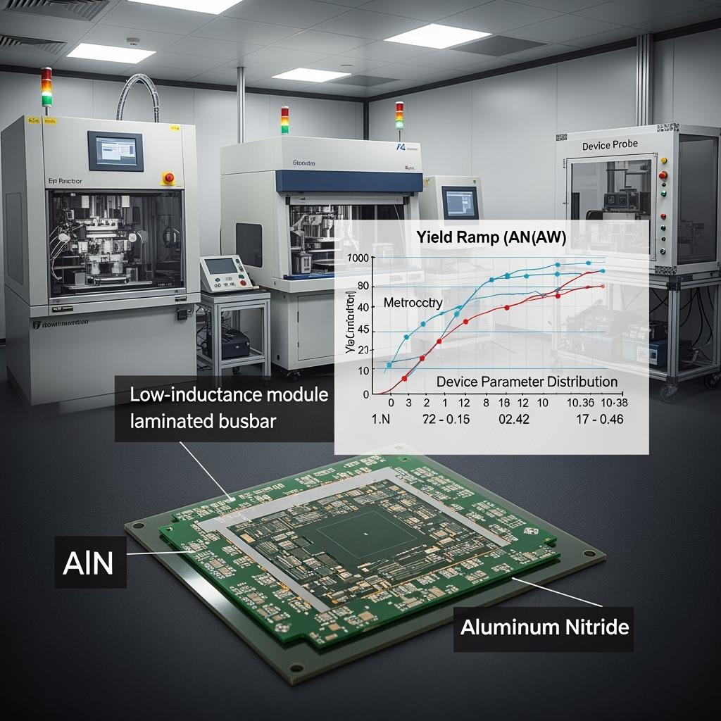
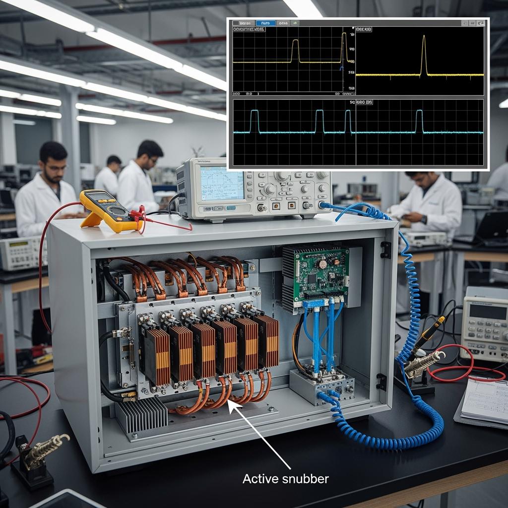
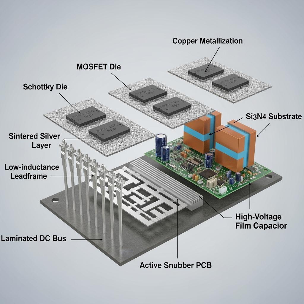
Module packaging cells integrate sintered-silver die attach and topside interconnects on copper-metallized AlN or Si3N4 substrates, with low-inductance leadframes and laminated busbars co-designed to target <10 nH loop inductance. Active snubber modules, low-ESR DC link capacitors, and automotive/plant-grade gate drivers complete the power stage. Post-packaging screening combines multi-temperature-zone electrical test with burn-in and accelerated reliability (power cycling, temperature cycling, high-temperature/high-humidity).
“Co-design across epitaxy, termination, gate dielectric, and packaging parasitics is where field performance is won or lost. When the loop is closed with inline data, iteration is measured in days—not quarters,” explains a Sicarbtech applications and yield engineering manager.
Performance Comparison: Localized SiC Pilot Platform vs Import-Only and Traditional Silicon
To guide decision-makers, the following comparisons highlight outcomes that affect yield, time-to-iteration, and downstream project success.
Pilot Manufacturing Outcomes for Pakistan’s Time-to-Market and Quality Needs
| Outcome in Local Use | Sicarbtech Local SiC Pilot Platform | Import-Only Silicon Carbide Supply | Conventional Silicon Devices and Packaging | Practical Impact |
|---|---|---|---|---|
| R&D iteration cycle (device-to-system) | Days to weeks with inline data | 6–12 weeks typical lag | Limited gains at lower frequency | Faster tuning for PQ/EMC; earlier COD |
| Wafer-to-wafer uniformity | ≤±2% thickness/doping targets | Vendor-dependent | 該当なし | Predictable device bins, easier matching |
| First-lot finished-goods yield | 80%–90% target with SPC | Not visible locally | High but lower performance | Stable small-batch supply |
| Packaging loop inductance | <10 nH co-designed | Vendor-dependent | 15–30 nH typical | Cleaner switching; smaller filters |
| Reliability screening (local HT/HH, power cycling) | In-country with shared datasets | Offshore; limited access | Variable; lower Tj | Stronger warranty evidence |
| Lead time volatility | Lower via local builds | High, FX/logistics sensitive | 中程度 | More reliable project delivery |
Real-World Applications and Success Stories: From Pilot to Product in Pakistan
A Lahore industrial park partnered with Sicarbtech to install a Phase I pilot covering epitaxy, wafer metrology, and device probe. Within three months, the team produced 1200 V samples with wafer uniformity within ±2%, then handed known-good-die to a local module packaging cell. A downstream energy storage converter prototype—destined for a textile mill—tested the modules and recorded an efficiency uplift of approximately one percentage point versus prior builds, while emissions passed on first utility inspection, shortening the acceptance cycle.
In Karachi, an EV charging OEM used the pilot’s quick-turn capability to evaluate gate-structure variants that tightened threshold-voltage spread by nearly half, improving current sharing and reducing overshoot during bidirectional operation. Prototype chargers passed conducted emission tests with comfortable margins, enabling lighter filters and a smaller cabinet footprint suited to roadside deployment.
A Faisalabad storage integrator collaborated on edge-termination recipes and snubber tuning for a 1700 V device module. With local HT/HH and power cycling, the team validated an extended warranty narrative acceptable to lenders. Time-to-iteration fell from a quarter to less than six weeks, aligning engineering cadence with customer commitments.
Technical Advantages and Implementation Benefits with Local Regulatory Alignment
Localized pilot capability transforms both the engineering and commercial trajectory of SiC programs in Pakistan. Epitaxy control reduces defect density and narrows device parameter distributions, improving matching and easing parallel operation—vital for storage converters and multi-module chargers. With local access to gate oxide and termination optimization, teams can tailor switching behavior and edge control to Pakistan’s feeder characteristics, shaving conducted and radiated emissions at the source.
On the packaging front, sintered-silver and ceramic substrates shorten thermal paths and extend power cycling life, retaining margin under hot, dusty, and humid conditions common in textile and steel corridors. Laminated busbars reduce loop inductance, which lowers ringing and overshoot; this, in turn, reduces snubber stress and filter size, improving reliability and cutting BOM cost. Local reliability screening—power cycling, temperature cycling, high-temperature/high-humidity—produces datasets that resonate with lenders and auditors. Moreover, end-to-end traceability gives owner’s engineers confidence during factory and site acceptance.
Comparative Portfolio View for Pilot-Line Decision-Makers
Mapping Pakistan’s Pilot-Line Requirements to Sicarbtech’s Integrated Offering
| Local Requirement | Epitaxy and Wafer | デバイス製造 | Module Packaging and Interconnect | Test, Reliability, and MES |
|---|---|---|---|---|
| Fast iteration, small-batch | CVD recipes with tight uniformity | Rapid gate/termination variants | Quick-turn sintered-silver modules | Inline probe; burn-in; SPC |
| High-yield ramp | Defect reduction, clean processes | Controlled implants/anneals | Low-inductance, robust assembly | Yield dashboards; traceability |
| PQ/EMC readiness | Uniform epi supports matching | Gate charge/threshold tuning | Laminated busbars <10 nH | On-site EMI pre-scan |
| Thermal reliability | Wafer flatness and k-consistency | Oxide integrity at Tj | AlN/Si3N4 + sintered silver | Power cycling; HT/HH |
| Local serviceability | Spare kits, training | Process updates | Rework and quick-swap designs | MES, genealogy, analytics |
Deep-Dive Engineering Comparison: SiC Pilot Stack vs Conventional Silicon Flow
Device, Packaging, and Process Parameters That Drive Field Performance
| パラメータ | Sicarbtech SiC Pilot Stack (Epi–Device–Module) | Conventional Silicon Flow | Operational Implication in Pakistan |
|---|---|---|---|
| Epi uniformity (thickness/doping) | ≤±2% targets | Wider spreads | Tighter device bins; better parallelism |
| Defect mapping to electricals | Inline correlation | Limited visibility | Faster root-cause and fixes |
| On-resistance and spread | −5% to −15% with tighter σ | Higher and broader | Lower conduction losses; predictable controls |
| Gate oxide integrity | Dedicated treatments | Generic | Stable high-frequency switching |
| Loop inductance | <10 nH (co-designed) | 15–30 nH | Cleaner edges; smaller filters |
| Junction–case thermal resistance | 0.05–0.12 °C/W | 0.10–0.20 °C/W | Lower hotspots; longer life |
| Sintered-silver interconnect | Standard | Solder | パワーサイクリングの堅牢性 |
| Reliability screening | Local HT/HH and cycling | Offshore | Bankable warranties |
| Iteration cadence | Days–weeks | Months | Faster PQ and firmware co-tuning |
Custom Manufacturing and Technology Transfer Services: Sicarbtech’s Turnkey Advantage
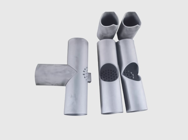
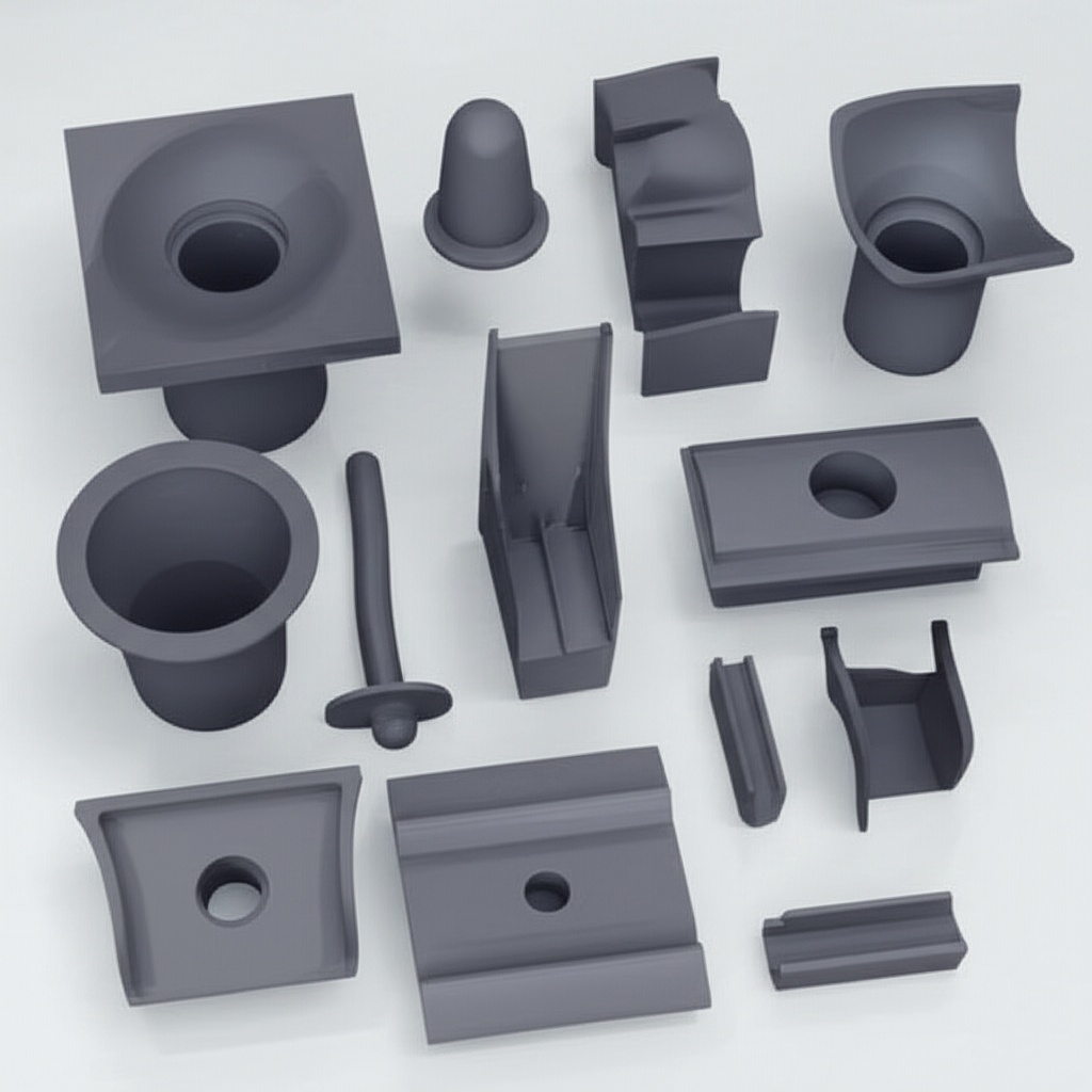
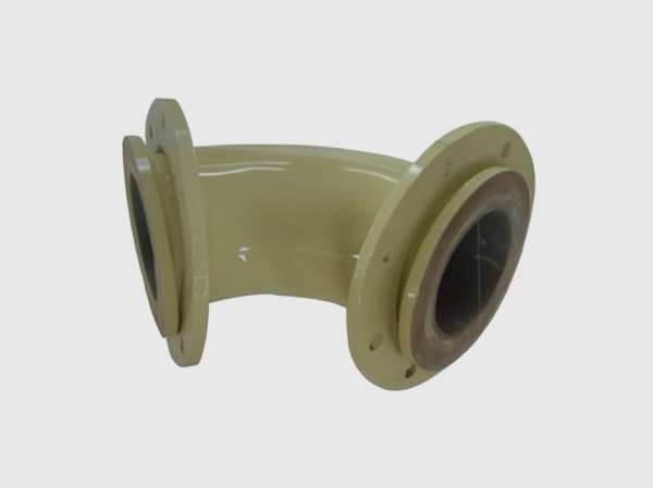
Sicarbtech stands apart by delivering not just equipment lists but a complete, taught process platform that yields predictable outcomes. Backed by the Chinese Academy of Sciences (Weifang) Innovation Park, Sicarbtech’s R&D and proprietary processes span R‑SiC, SSiC, RBSiC, and SiSiC ceramic grades that anchor thermal conductivity and mechanical robustness in module substrates and fixtures. The transfer does not end with installation; it embeds a measurement culture.
The technology transfer package includes:
- Process know-how for epitaxy, including CVD recipes aligned to 1200/1700 V targets with defect-density reduction tactics; wafer thinning/polishing controls for TTV and roughness; ion implantation and anneal windows that balance junction depth with leakage.
- Device fabrication guidance across edge termination and gate dielectric treatments to reduce interface states and leakage while preserving high-frequency switching quality.
- Packaging co-design methods covering sintered-silver die attach and topside interconnects, copper-metallized AlN/Si3N4 substrate selection, and laminated busbar geometry to achieve <10 nH loops.
- Equipment specifications for utilities and cleanroom infrastructure, sintering presses, dicing/bonding tools, plasma etchers, metallization and anneal furnaces, IP/leak testing, active snubber calibration, and parasitic/thermal metrology.
- Training programs for operators, process and test engineers, quality teams, and application engineers—emphasizing statistical process control, inline metrology, accelerated stress testing (power cycling, temperature cycling, HT/HH), and EMI/thermal co-design.
- Factory establishment services from feasibility studies tuned to Pakistani utilities and labor, through pilot-line installation, qualification lots, and yield ramp with SPC dashboards and reaction plans.
- Quality systems integration: ISO 9001 and ISO 14001 alignment, MES and genealogy deployment for batch traceability, and support for relevant IEC/UL component and converter certifications as demanded by downstream PV, storage, and EV programs.
- Ongoing technical support and process optimization: quarterly audits, recipe and window updates, reliability dataset refreshes, and on-call application engineering to translate device/package improvements into system-level gains.
“Scaling SiC is a metrology discipline: what you measure every shift is what you can improve every quarter. That is how you move from hero lots to a stable pilot,” says a Sicarbtech process transfer leader. With 10+ years of customization and 19+ enterprise collaborations, Sicarbtech brings a repeatable, low-risk pathway from first wafer to field-proven modules.
Future Market Opportunities and 2025+ Trends: Building a Sustainable SiC Ecosystem
Pakistan’s industrial sectors will increasingly demand high-efficiency, grid-friendly power conversion with short lead times. Localized pilots will catalyze three parallel dynamics. First, downstream system OEMs will iterate faster on PQ, EMC, and thermal designs, improving first-pass interconnection success and compressing COD timelines. Second, the knowledge base—process parameters, inline metrics, and reliability datasets—will reduce dependency on external cycles and enable confident long-term warranties. Third, a modular pilot architecture will ease expansion to additional voltage classes and device types, including trench gate evolutions and extended edge-termination schemes.
Trends to watch include closer coupling between device/package parasitics and digital control strategies, enabling even smaller filters and faster dynamic response; greater use of laminated busbar standards across product families to speed module swaps; and integration of condition-based monitoring not just in systems but within pilot lines to preempt drift. We expect SiC penetration across mid-to-high-end converters in Pakistan to move toward 30–50% through the next few years, with localized pilot capacity becoming a procurement lever for EPCs and operators focused on time-to-revenue and lifecycle economics.
よくある質問
What performance and yield gains are realistic when standing up a SiC pilot line locally?
Teams commonly achieve wafer uniformity within ±2%, reduce device on-resistance by 5–15% with tighter distribution, and raise first-lot finished-goods yield into the 80–90% range. System-level efficiency gains of around one percentage point are typical when device/package co-optimization feeds downstream designs.
How does Sicarbtech shorten iteration from device changes to system validation?
We align epi, device, and packaging windows with inline electricals and fast handoff to local module cells. That lets system teams validate PQ, EMC, and thermal behavior within days to weeks, rather than months, using shared metrology and genealogy.
What equipment and facilities are essential for a Phase I pilot?
Core tools include a CVD epi reactor, wafer thinning/polish, ion implantation and anneal, plasma etch for trenches and terminations, oxide growth/treatments, metallization/anneal, electrical probe, dicing/sorting, a sintered-silver module cell with AlN/Si3N4 substrates and laminated busbars, and reliability bays for power and temperature cycling and HT/HH.
Can the pilot line support both 1200 V and 1700 V platforms?
Yes. Recipes and masks are configured for both platforms, and equipment headroom is specified to accommodate trench and advanced termination structures as your roadmap evolves.
How do you ensure PQ/EMC readiness for Pakistan’s weak feeders?
We co-design low-parasitic packaging (<10 nH loops) and provide edge-rate control through gate drivers. Combined with active snubbers and right-sized filters, systems routinely achieve ≤3% THD and near-unity PF, easing interconnection.
What reliability evidence resonates with lenders and insurers?
Local power cycling at elevated junction temperatures, temperature cycling, high-temperature/high-humidity, and dust/salt-mist exposure—paired with telemetry from prototypes—create a compelling warranty basis. We provide datasets and test plans aligned with these stressors.
How long from contract to first articles on a pilot line?
Typical timelines are a few months, depending on facility readiness and import logistics for key tools. We stage equipment installation and bring-up to enable early learning on metrology and front-end steps before full packaging and reliability come online.
What local skills and staffing are required?
A core team includes process integration, epi/device engineers, packaging engineers, test and reliability engineers, and manufacturing/quality specialists. We provide comprehensive training, SOPs, and SPC frameworks to accelerate competence.
Can Sicarbtech integrate MES and traceability from day one?
Yes. We deploy MES and genealogy tailored to pilot-scale volumes, enabling batch-level traceability across epi–wafer–device–module–test. Data models support rapid root-cause and continuous improvement.
How does the pilot position us for volume scale-up?
We design modular, portable process architectures. Once windows are stable, recipes and control plans transfer to added lines or partners with minimal re-qualification, preserving yield and electrical distributions.
オペレーションに適した選択
The strongest pilot programs start with clarity on downstream products, interconnection requirements, and site conditions. Map your 1200/1700 V device mix, target converters (PV, storage, EV charging), and PQ/EMC objectives against facility readiness, staffing, and budget. When Sicarbtech co-designs from CVD recipes and gate-oxide treatments through termination, parasitics, laminated busbars, and thermal paths, the benefits compound: faster iteration, higher yield, cleaner switching, cooler modules, and stronger acceptance narratives. For textile mills seeking resilient storage, cement and steel plants integrating PV and fast charging, and EV networks scaling across cities, a local SiC pilot platform turns schedule risk into competitive advantage.
専門家によるコンサルテーションとカスタムソリューション
Whether you are planning a greenfield pilot or upgrading an existing line, Sicarbtech will translate your roadmap into a stepwise implementation plan with milestones for facility, process windows, yields, and downstream validation. Contact: [email protected] | +86 133 6536 0038.
記事のメタデータ
Last updated: 2025-09-17
Next scheduled review: 2025-12-01
Content freshness indicators: 2025 Pakistan SiC pilot manufacturing outlook; 1200/1700 V device platforms; epi–device–module co-design; sintered silver and AlN/Si3N4 substrates; laminated low-parasitic busbars; inline SPC and MES traceability; local HT/HH and cycling reliability; case narratives in Lahore, Karachi, and Faisalabad.
About Sicarbtech: Silicon Carbide Solutions Expert located in Weifang City, China’s silicon carbide manufacturing hub; member of Chinese Academy of Sciences (Weifang) Innovation Park; 10+ years of SiC customization; supporting 19+ local enterprises with advanced SiC technology; full-cycle solutions from material processing to finished products; specializing in R‑SiC, SSiC, RBSiC, and SiSiC grade products; services include custom manufacturing, factory establishment, and technology transfer.

About the Author: Sicarb Tech
We provide clear and reliable insights into silicon carbide materials, component manufacturing, application technologies, and global market trends. Our content reflects industry expertise, practical experience, and a commitment to helping readers understand the evolving SiC landscape.