高度な熱管理と高電力密度を実現するSiCチップレベル・ヒートスプレッダー基板
シェア
製品概要と2025年の市場関連性
SiCチップレベル・ヒートスプレッダー基板は、半導体ダイの直下やパワーモジュールのスタック内に配置され、熱を伝導して横方向に拡散させ、熱勾配とピーク接合部温度を低減させるセラミック部品です。反応焼結SiC(RBSiC)、無圧/固体焼結SiC(SSiC)、SiSiCハイブリッドなどを使用することで、これらの基板は高い熱伝導性、優れた剛性、耐食性を実現します。パキスタンの繊維、セメント 鉄鋼 これらの材料は、高温、埃っぽい、グリッドが不安定な環境において、より高いスイッチング周波数、より高い電力密度、より長い寿命を可能にします。
なぜ2025年が採用にとって極めて重要なのか:
- UPS、VFD、PV/BESS用のコンパクトな高密度コンバータには、高い周囲温度(40~45℃)で97%以上の効率を維持するための積極的な熱設計が必要です。
- 局所的なグリッドのたるみ/うねりや頻繁なサイクルは熱機械疲労を加速させるが、優れた熱拡散がΔTjを低減し、信頼性を向上させる。
- データホールやMCCルームでは、スペースと設備投資費用が逼迫しており、ヒートシンクの小型化と静音化が求められています。
- RBSiC/SSiC基板は、AlN/Si3N4 DBCスタックや銀焼結ダイアタッチとシームレスに統合され、175~200℃までのSiCデバイスの信頼性の可能性を最大限に引き出します。
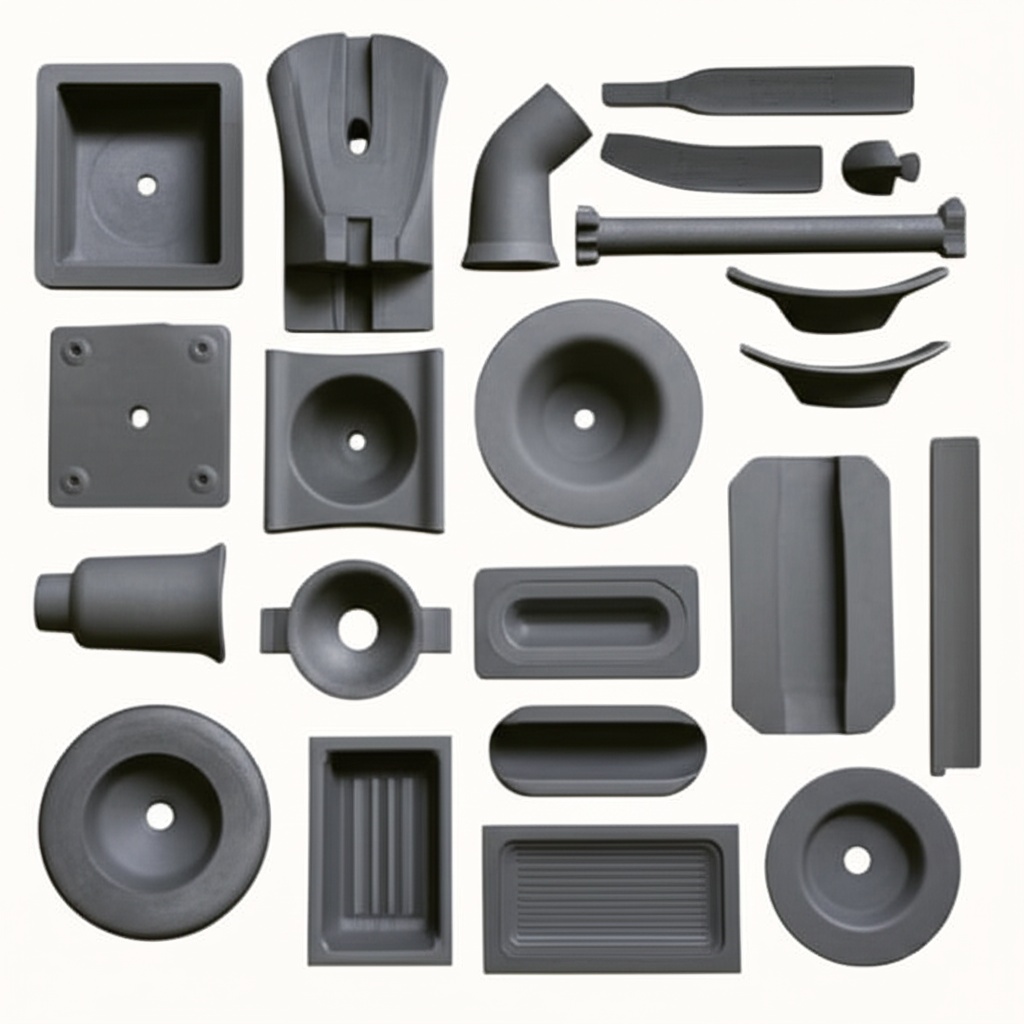
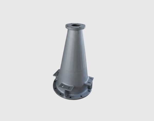
Sicarb Techは、ディスクリートパッケージ(TO-247/TO-263)、ハーフブリッジ/フルブリッジモジュール、インテリジェントパワーブロック用にカスタマイズされたチップスケールスプレッダーとモジュールスケールベースインサートを提供しています。
技術仕様と高度な機能
代表的な機能(デバイス/モジュールごとにカスタマイズ):
- 材料と熱特性
- SSiC:高純度、高強度、熱伝導率は通常150~200W/m・K、優れた耐摩耗性/耐食性
- RBSiC: コスト効率に優れ、高い熱伝導性を発揮。
- SiSiC:導電性とCTEを調整するシリコン浸透構造
- 機械および寸法
- 厚さ:0.2~2.0mmチップインサート、2~6mmモジュールインサート/ベースプレート
- 平坦度:モジュールフットプリント全体で50 µm以下、局所チップゾーンで20 µm以下
- 表面仕上げ:TIMと焼結界面を最適化するためRa≤0.4 µm
- AlN/Si3N4 DBCとのCTEマッチングにより応力を最小化
- 統合とインターフェース
- 銀焼結はんだ、TLPはんだ、高信頼性はんだに対応
- ボンディングや電気シールドに必要なメタライゼーションオプション(Ti/Ni/Ag)
- ワイヤー・ボンドレス銅クリップ・アセンブリおよびケルビン線ソース・レイアウトに対応
- 熱性能目標
- RθJCの削減:10~25%対非拡散スタック(アプリケーションに依存)
- ΔTjの低減:50~100 kHzのスイッチングで高フラックスのホットスポットで8~20 K
- パルス負荷と電力サイクルに対するZth(j-a)過渡応答の改善
- 環境的堅牢性
- セメント/テキスタイル用の耐塵性/耐摩耗性、コンフォーマルコーティングおよび密閉型エンクロージャーとの適合性
- 液冷適合性:腐食防止剤との相溶性に優れ、流動下での浸食が少ない。
- コンプライアンスの調整
- IEC 60664 絶縁調整(スタックレベル)、IEC 60068 環境試験、IEC 62477-1 安全性; PEC および NTDC 実習
シカーブ・テックのエンジニアリング・サービス:
- ミッションプロファイルに基づく電力損失マップを用いた熱FEA
- IRサーモグラフィーの相関と熱量測定による検証
- センサー埋め込み用のカスタム加工とレーザー機能(NTC/RTD/ファイバーブラッグ)
産業用パワーエレクトロニクスのための測定可能な熱と密度の向上
| パキスタンのホットサイトにおける接合部温度上昇の低減と高密度化 | SiCチップレベルヒートスプレッダ基板(Sicarb Tech) | 従来の銅スラグ/アルミスプレッダー |
|---|---|---|
| 熱伝導率とホットスポットの広がり | SiCセラミックスとの高い拡散性、高Tで安定 | 中程度;局所的なホットスポットが続く |
| パルス負荷時のΔTj | -8~-20 K 典型的な改善 | ベースライン |
| サイクリング下での信頼性 | 高い(硬い、低疲労、良好なCTEペアリング) | 中;CTEミスマッチのリスク |
| 耐食性/耐塵性 | 摩耗性/粉塵の多い環境で優れている | 可変;酸化と摩耗の懸念 |
| ヒートシンクとファンのサイズ | Rθ経路の低下により減少 | ホットスポットを補正するために大きくなっている |
主な利点と実証済みのメリット
- ジャンクション温度と勾配を低減:ダイ下のスプレッダー・インサートが熱ピークを低減し、パキスタンの頻繁な電圧変動と周囲熱の下での寿命を延ばします。
- 電力密度の向上:ホットスポットを緩和することで、設計者はスイッチング周波数と電流密度を押し上げ、磁気回路とヒートシンクを縮小することができます。
- 過酷な環境下での信頼性セラミック強度と耐摩耗性により、粉塵の多いセメント工場や繊維工場での劣化を防ぎます。
- コストとOPEXの節約:冷却システムの小型化、TIMの長寿命化(ポンプアウトの減少)、サーマルトリップの減少により、メンテナンスとエネルギーコストが削減されます。
専門家の言葉を引用する:
「高導電性セラミックと先進的なアタッチメントを使用したダイレベルでの局所的な熱管理は、高い接合温度でSiCの信頼性を実現するために不可欠となっています。- IEEEパワーエレクトロニクス誌、WBGにおけるパッケージングと熱トレンド、2024年
実際のアプリケーションと測定可能な成功事例
- ラホールデータセンターUPSインバーターモジュール:
- 高損失スイッチの下に埋め込まれたSSiCチップレベル・スプレッダ。
- 結果UPS全体の効率は97.3%に達し、冷却ファンの速度プロファイルが低下し、空調エネルギーを約9%節約した。
- ファイサラバードの繊維VFDフレーム:
- RBSiCベースインサートは、コンフォーマルコートされたPCBを持つハーフブリッジモジュールの下に挿入されます。
- 結果キャビネット温度が18%低下し、夏季のサーマル・トリップが20%減少。
- カラチの鋼製補助ポンプ:
- SiSiCハイブリッドスプレッダと銀焼結アタッチメント。
- 性能:パワーサイクリングモデルから22~28%の寿命延長を予測。
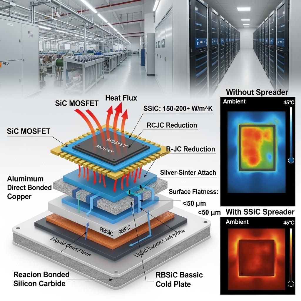
【画像プロンプト:詳細な技術説明】 100 kHzでのサイドバイサイドの熱マップ:左はチップレベルスプレッダーなしのモジュールで集中したホットスポットを示し、右はSSiCスプレッダー付きのモジュールで均一な熱分布を示す。ダイ-焼結体-DBC-SiCスプレッダ-TIM-コールドプレートのスタックの分解図を含み、厚さ、導電率、ΔTjの改善が示されている。フォトリアリスティック、4K。
選択とメンテナンスの考慮事項
- 素材の選択
- 予算が許す限り、最大限の導電性と機械的強度を得るにはSSiCを、強力な性能でコストを最適化するにはRBSiCを、CTE調整が必要な場合はSiSiCをお選びください。
- スタック統合
- 平坦度と表面仕上げの目標値を確認する。175~200℃で最高の熱/老化性能を得るために銀焼結を指定する。
- 振動とサイクルレベルに基づいてDBC材料(高誘電率はAlN、靭性はSi3N4)を検証する。
- 冷却戦略
- 250 kWを超えるキャビネットまたは高地では、液冷を検討する。コールドプレートを保護するため、水の化学的性質(pH、抑制剤)を管理する。
- TIMの厚さを100μmに保ち、ポンプアウトを監視する。相変化グリースまたは高安定性グリースを選択する。
- 環境保護
- 粉塵の多い環境では、コーティングと正圧エンクロージャを使用すること。ガスケットとシールの完全性を確認すること。
- 検証とQA
- IRサーモグラフィと過渡Zth測定を実施し、FEAと相関させる。
- パイロット運転でΔTjの傾向を追跡し、それに応じてスプレッダーの厚さと設置面積を調整する。
業界の成功要因と顧客の声
- 成功要因:
- より高いスイッチング周波数を利用するための磁気学およびレイアウトとの早期熱共同設計
- パキスタンのグリッドサグとアンビエントピークを反映したミッションプロファイルに基づく損失マッピング
- 平坦度、粗さ、付着気孔率の厳密な計測
- 最も暑い時期にパイロット検証を行い、マージンを確認する。
- 証言(パンジャブ州の大手セメントメーカー、オペレーション・マネージャー):
- 「チップレベルのSiCスプレッダーは、ホットスポットを平らにし、夏のピーク時のドライブを安定させました。メンテナンスウィンドウは短くなり、頻度も減りました。
将来のイノベーションと市場トレンド
- 2025~2027年の見通し:
- SiCスプレッダとマイクロチャンネルコールドプレートを組み込んだ両面冷却モジュール
- 200 mm SiCウェハのエコシステムにより、デバイスコストを低減し、高度なパッケージングの幅広い採用を可能にする
- スプレッダー内にセンサー(ファイバーブラッグ/RTD)を内蔵し、リアルタイムの温度マッピングと予知保全を実現
- SiCセラミックスとグラファイトプレーンを組み合わせたハイブリッド複合材料による極端な横方向への広がり
業界の視点:
「熱工学は現在、WBGシステムの電力密度を高めるための主要な手段であり、セラミックスプレッダが中心的な役割を果たしている。- IEA技術展望2024、パワーエレクトロニクスの章
よくある質問と専門家による回答
- ΔTjの低減はどの程度期待できますか?
- 損失分布、スプレッダーの厚さ、冷却方法によって異なるが、通常8~20K。
- スプレッダーを付けると熱抵抗は増えますか?
- 適切に設計された場合は違います。高誘電率SiCセラミックと銀-焼結界面は、横方向の分布を改善しながら、全体のRθJCを低減します。
- スプレッダーは既存のモジュールと互換性がありますか?
- はい、DBCの下のインサートとして、またはベースプレートのアップグレードとして。スタックの高さを維持するための加工や厚みのオプションを提供します。
- スプレッダーは電気絶縁に影響しますか?
- スプレッダーは機械-熱スタックの一部であり、電気的絶縁はIEC 60664に準拠したDBCセラミックと絶縁体を介して保たれる。
- ROIとは?
- エネルギー、冷却、メンテナンス間隔の延長により、連続稼動のUPS/VFDアプリケーションで12~24ヶ月。
このソリューションがお客様の業務に役立つ理由
SiCチップレベル・ヒートスプレッダー基板は、ホットスポットを削減し、接合部温度を安定化させ、より高いスイッチング周波数を可能にすることで、パキスタンの熱と環境に関する課題に直接対応します。これは、繊維、セメント、鉄鋼、および新興のデータ・インフラストラクチャにおいて、より高密度で静かな、より効率的なUPSおよびドライブ・システムの長寿命化とトリップの低減という中核的な利点につながります。
カスタムソリューションについては専門家にご相談ください
シカーブ・テックでサーマル・スタックを強化:
- 中国科学院の支援による10年以上のSiC製造専門知識
- R-SiC、SSiC、R
- ローカルでの価値創造のための技術移転と工場設立サービス
- 材料加工から完成した検証済みのサーマル・スタックまでのターンキー・ソリューション
- ラピッドプロトタイピング、IR/FEA相関、パイロット導入など、19社以上の企業との実績。
コンバーターの熱監査、ΔTj削減の見積もり、ROIモデルを無料で入手できます。
- Eメール:[email protected]
- 電話/WhatsApp:+86 133 6536 0038
2025年第4四半期のエンジニアリングおよび生産枠を確保し、夏のピーク負荷の前に供給を確保する。
記事のメタデータ
- 最終更新日:2025年9月11日
- 次回のレビュー:2025-12-15
- 著者シカーブ・テック・パッケージング&サーマル・エンジニアリングチーム
- Contact: [email protected] | +86 133 6536 0038
- 規格の焦点:IEC 60664、IEC 62477-1、IEC 60068; PEC慣行およびNTDCグリッドコード品質基準に沿ったもの。

About the Author: Sicarb Tech
We provide clear and reliable insights into silicon carbide materials, component manufacturing, application technologies, and global market trends. Our content reflects industry expertise, practical experience, and a commitment to helping readers understand the evolving SiC landscape.