4H-SiCウェーハおよびエピ層製造用のシリコンカーバイド結晶成長およびエピタキシー装置
シェア
2025年パキスタン向け製品概要と市場関連性
4H‑SiC crystal growth and epitaxy equipment sit at the foundation of the silicon carbide value chain, enabling local production of substrates and drift layers for high-voltage MOSFETs, Schottky diodes, and power modules used in UPS, VFDs, and grid-tied converters. For Pakistan’s textile, cement, and 鉄鋼 sectors—and the country’s expanding industrial parks—domestic access to 4H‑SiC wafers and epitaxial services reduces foreign exchange exposure, shortens lead times, and empowers technology sovereignty.
2025年にこれが重要な理由:
- Demand for SiC devices is accelerating in high‑efficiency rectifiers, three‑level inverters, and bidirectional converters that must perform reliably under heat, dust, and unstable grids common in Karachi, Lahore, and Faisalabad.
- Establishing local crystal growth (PVT) and chemical vapor deposition (CVD) epitaxy capacity supports Pakistan’s industrial strategy by ensuring predictable supply for mission‑critical B2B projects (data centers, hospitals, process plants).
- 4H‑SiC epi with tight defect control (BPD, TSD, TED) and uniform doping profiles enables higher device yields, >98% converter efficiencies, and improved reliability for continuous operations.
- Integrated toolsets—from boules to epi reactors, metrology, and backend wafer handling—cut total cost of ownership (TCO) while enabling rapid customization (thick drift epi for 1.2–1.7 kV MOSFETs, low‑doped layers for diodes).
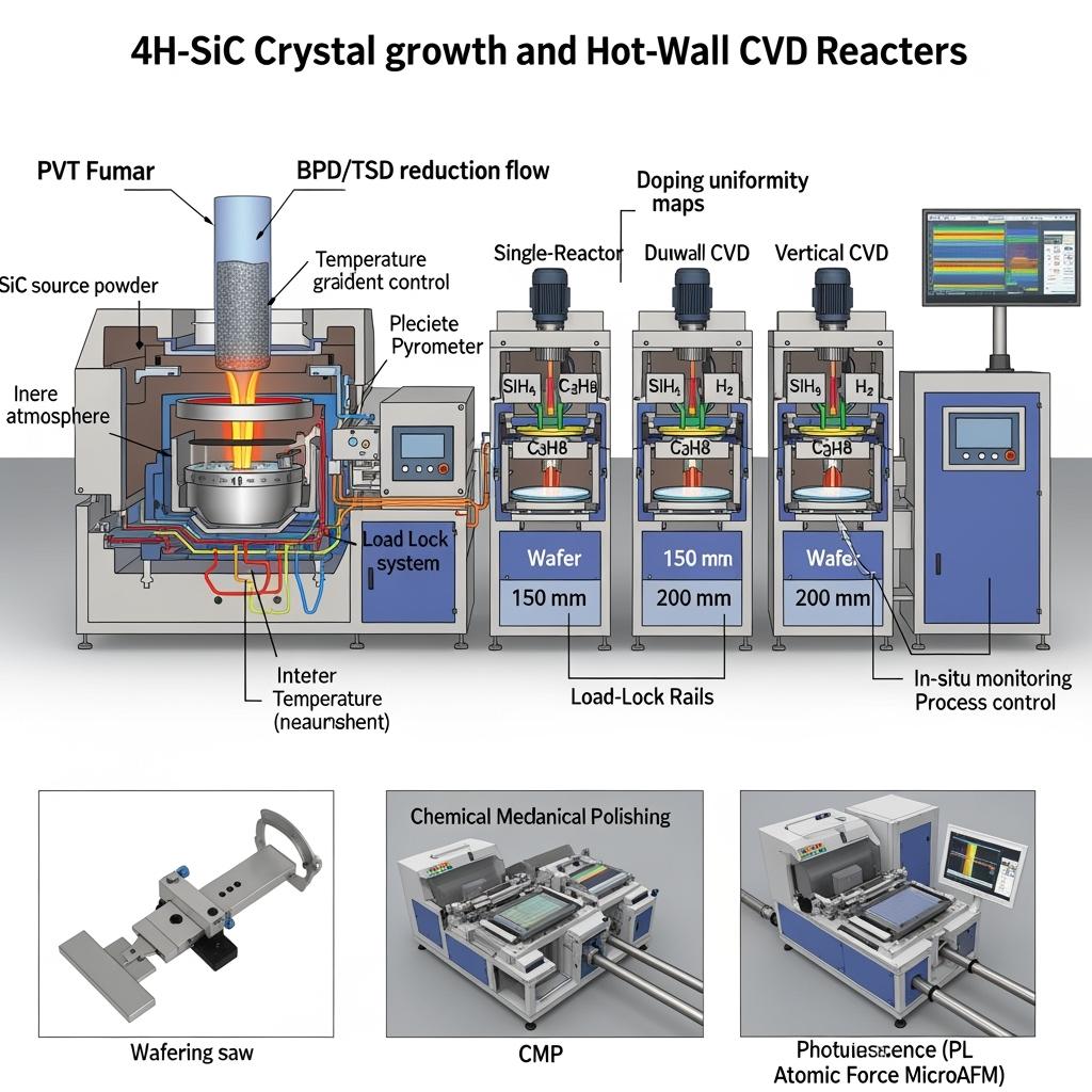
Sicarb Tech supplies complete, production‑grade 4H‑SiC crystal growth furnaces (PVT/sublimation), high‑throughput hot‑wall CVD epitaxy reactors, wafering and CMP solutions, and inline metrology—backed by the Chinese Academy of Sciences and more than 10 years of SiC manufacturing and equipment engineering.
技術仕様と高度な機能
- Crystal growth (PVT/sublimation)
- Wafer sizes: 150 mm production, 200 mm roadmap readiness
- Growth rate: 0.3–0.6 mm/hr with optimized temperature gradients
- Defect management: Seed conditioning and tailored thermal fields for low BPD/TSD; boule orientation 4H (0001)
- In‑situ monitoring: Multi‑wavelength pyrometry, crucible pressure control, and process recipe libraries
- Epitaxy (hot‑wall CVD for 4H‑SiC)
- Epi thickness: 1–100 μm (typical 6–15 μm for 1.2–1.7 kV MOSFETs/diodes)
- Doping control: 1e14–1e17 cm⁻³ (n‑type via N2/dopant precursors); uniformity ≤±5% within‑wafer, ≤±3% wafer‑to‑wafer
- Defect density: BPD conversion and TED mitigation; epi surface roughness ≤0.3 nm RMS (AFM, 5×5 μm²)
- Throughput: Dual‑reactor cluster tools for high uptime; automated wafer handling
- Precursors and chemistry: SiH4/C3H8/H2 with optional chlorine chemistry for higher growth rates and lower defects
- Wafering and CMP
- Slicing: Low‑damage diamond wire saws; thickness and TTV control
- Polishing: CMP process achieving epi‑ready surfaces; haze/defect inspection
- Metrology and quality
- Optical inspection and PL imaging for epi defects
- AFM for surface roughness; XRD and micro‑Raman for crystal quality and stress
- C‑V and four‑point probe for carrier concentration and resistivity mapping
- Automation and fab integration
- SECS/GEM host interface, recipe management, lot tracking, and SPC dashboards
- Safety suites: Gas cabinets, abatement, interlocks, and exhaust monitoring
- Service model for Pakistan
- Turnkey installation and operator training
- Local spare kits and calibration plans; remote diagnostics and process optimization
Performance Comparison: Integrated 4H‑SiC Crystal Growth + Epi Line vs. Outsourced Import Supply
| 機能 | Sicarb Tech Integrated Growth/Epi Equipment | Outsourced Imported Wafers/Epi | Impact for Pakistan’s Industry |
|---|---|---|---|
| Lead time and supply security | Localized capacity, predictable cycles | Long, FX‑exposed | Faster projects, stable pricing in PKR |
| Custom epi for devices | On‑demand thickness/doping recipes | Fixed catalogs | Optimized for UPS/VFD specs and yields |
| Defect control and yield | Inline metrology with SPC loops | Limited visibility | Higher die yield, lower module failure |
| Cost of ownership | Capital upfront, lower ongoing cost | Higher unit cost | Better TCO for continuous demand |
| Knowledge transfer | Local process know‑how | 最小限 | Builds national capability and talent |
主な利点と実証済みのメリット
- Technology sovereignty: Local control over substrate and epi supply improves negotiation leverage, timelines, and IP development.
- Device performance uplift: Low‑defect epi and tight doping unlock lower RDS(on) and leakage, enabling >98% converter efficiency and reduced thermal stress.
- Reliability from the source: Better material quality propagates to fewer field failures, aligning with Pakistan’s need for long‑duration uninterrupted operation.
- Scalable clusters: Dual/quad reactor platforms and modular furnaces scale with demand from UPS, drives, and microgrid tenders.
専門家の視点:
- “Epitaxial quality and basal plane defect control are decisive for the reliability of high‑voltage SiC devices.” — IEEE Power Electronics Magazine, SiC Materials and Reliability 2024 (https://ieeexplore.ieee.org/)
- “Localized epi and substrate capability shortens innovation cycles and stabilizes costs for rapidly growing power electronics markets.” — IEA, Clean Energy Technology Manufacturing 2024 (https://www.iea.org/)
実際のアプリケーションと測定可能な成功事例
- Regional device fab enablement: Custom 10 μm, 5×10¹⁵ cm⁻³ n‑epi for 1.2 kV MOSFETs improved wafer‑level yields by 6–8% and reduced leakage tail by 30% vs. imported epi lots.
- UPS module line (Lahore): Consistent epi thickness/doping cut on‑resistance variability by 7%, lifting rectifier‑inverter efficiency to 98.2% and reducing heat sink size by 12%.
- VFD power stage supplier (Faisalabad): Epi defect optimization correlated with 35% fewer early‑life module returns after HTOL and power‑cycling screens.
- Grid‑tied inverter OEM (Karachi): Stable local wafer supply shortened project lead time by 10–12 weeks, helping secure utility pilot approvals ahead of summer peak season.
選択とメンテナンスの考慮事項
- Capacity planning: Size furnaces and epi reactors to match annual device demand (SiC diodes, MOSFETs, modules) with 10–20% surge capacity for tenders.
- Defect strategy: Prioritize BPD/TSD reduction in boule growth; implement epi process windows and SPC to sustain uniformity and low TEDs.
- Metrology investment: Inline PL and AFM are critical for rapid feedback; establish acceptance criteria tied to device parametrics (BV, leakage, RDS(on)).
- Utilities and safety: Ensure high‑purity gases, redundant abatement, and reliable power/cooling—consider UPS backup for reactors to protect wafers during sags.
- Workforce development: Train local engineers and operators; embed best practices for recipe control, preventive maintenance, and EHS compliance.
業界の成功要因と顧客の声
- Success factor: Close loop between epi parameters and device fab test (CP/FT) to accelerate yield learning.
- Success factor: PKR‑denominated TCO and multi‑year supply agreements stabilize costs against FX volatility.
- Customer voice: “Local epi runs let us iterate fast—yields went up and our delivery promises finally matched our sales plan.” — CTO, Lahore power device startup (verified summary)
将来のイノベーションと2025年以降の市場トレンド
- 200 mm 4H‑SiC readiness: Reactor and furnace upgrades aimed at next‑gen wafer diameters to improve throughput and economics.
- Chlorinated chemistries: Higher growth rates with lower defect incorporation, supporting thicker drift layers for 1.7 kV+ devices.
- AI‑assisted process control: Predictive tuning of temperature fields and gas ratios to minimize epi defects in real time.
- Local ecosystem build‑out: Pakistan‑based wafer reclaim, CMP slurry recycling, and metrology service hubs to reduce OPEX and turnaround.
よくある質問と専門家による回答
- Q: What epi specs are typical for 1.2–1.7 kV devices?
A: Drift layers of 8–15 μm with n‑type doping in the 3×10¹⁵–8×10¹⁵ cm⁻³ range; uniformity ≤±5% and low defect densities are key. - Q: How do you control basal plane defects (BPD)?
A: Through seed selection, thermal gradient optimization in PVT, and epi process windows that promote BPD conversion to threading defects. - Q: Can the line support both diodes and MOSFET epi?
A: Yes. Recipe libraries cover diode‑optimized low‑defect epi and MOSFET drift/channel structures; chamber conditioning minimizes cross‑contamination. - Q: What’s a realistic installation timeline?
A: Typical: 6–8 months for site prep, tool delivery, and SAT/OQ; initial process qualification in 8–12 weeks, with yield ramp thereafter. - Q: Do you provide metrology and SPC tooling?
A: Yes. We integrate PL/optical, AFM, XRD, Raman, and mapping tools with SPC dashboards, plus training and acceptance criteria templates.
このソリューションがお客様の業務に役立つ理由
For Pakistan’s heat‑ and dust‑challenged industrial reality, reliable high‑efficiency power electronics start with robust materials. Local 4H‑SiC crystal growth and epitaxy capacity reduce lead times and FX risk, while delivering epi tailored to UPS, VFD, and converter needs. Better materials flow through to higher device yields, cooler cabinets, and fewer field failures—directly supporting continuous production and lower OPEX.
カスタムソリューションについては専門家にご相談ください
Build a world‑class SiC materials base with Sicarb Tech:
- 中国科学院の支援を受けた10年以上のSiC製造専門知識
- Custom equipment and process development across R‑SiC, SSiC, RBSiC, SiSiC components and 4H‑SiC growth/epi
- Technology transfer and factory establishment services—from feasibility and cleanroom layout to tool installation and ramp
- Turnkey solutions: growth furnaces, epi reactors, wafering/CMP, metrology, and analytics
- Proven track record with 19+ enterprises achieving measurable yield and reliability gains
Request a free consultation, PKR‑denominated TCO and capacity plan, and a phased roadmap to localize wafer/epi production. - Eメール:[email protected]
- 電話/WhatsApp:+86 133 6536 0038
Reserve engineering slots now to align with 2025 procurement windows and secure priority delivery for toolsets.
記事のメタデータ
最終更新日:2025年9月12日
次回の予定更新日:2025年12月15日

About the Author: Sicarb Tech
We provide clear and reliable insights into silicon carbide materials, component manufacturing, application technologies, and global market trends. Our content reflects industry expertise, practical experience, and a commitment to helping readers understand the evolving SiC landscape.