SiC MOSFET用に最適化された高周波、高温ゲートドライバ(絶縁、高dv/dt耐性)
シェア
パキスタンの2025年における高効率コンバータのゲートドライブ信頼性
パキスタンの繊維、セメント、および 鉄鋼 シンド州とバロチスタン州で再生可能エネルギー容量が拡大する中、各セクターは電化と電力品質の向上を加速させています。SVG/STATCOM、APF、高周波ドライブ、UPS、および産業用電源におけるSiC(Silicon Carbide)MOSFETの効率と速度を最大限に実現するには、ゲートドライバがミッションクリティカルです。高周波、高温のSiC最適化ゲートドライバは、強化された絶縁と高いdv/dt耐性を備え、誤ったターンオンを防ぎ、スイッチング損失を最小限に抑え、45°Cを超える周囲温度、ほこり、および湿度下での安定した動作を保証します。
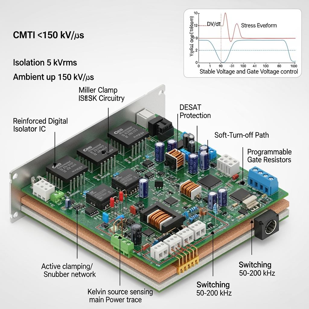
Sicarb Techは、堅牢な絶縁、広いコモンモード過渡耐性(CMTI)、精密なミラー制御、およびプログラム可能なターンオン/ターンオフダイナミクスを特徴とするSiC最適化ゲート駆動ソリューションを設計および供給しています。中国科学院の支援を受けて、当社のプラットフォームはマルチレベルトポロジとIEC 61850監視システムにシームレスに統合され、NTDC/NEPRA相互接続の試運転サイクルを短縮し、長期的な信頼性を向上させます。
技術仕様と高度な機能
- 絶縁とノイズ耐性
- 最大5 kVrmsの強化絶縁; IEC 60664-1に準拠した沿面距離/空間距離
- データ破損なしで高速SiCスイッチングエッジに耐えるCMTI≥150 kV/µs
- 変電所や工場での長くてノイズの多いケーブル配線用の光ファイバーまたは差動リンクオプション
- ゲート制御と保護
- EMIとオーバーシュート制御のためのプログラム可能なゲート抵抗と分割RG(ターンオン/ターンオフ)
- 誤ったターンオンを防ぐためのミラークランプと負のゲートバイアス(例:+18 V / −3〜−5 V)
- ソフトターンオフ付きDESAT過電流保護; 短絡耐性調整
- アクティブゲート制御プロファイル:損失とEMIのバランスを取るためのdi/dtとdv/dtシェーピング
- 電源と熱
- 絶縁バイアス電源±18 Vクラス、チャネルあたり3〜6 W; SiC MOSFET要件に適合するUVLOしきい値
- 最大105°Cの周囲温度で動作; 産業グレードに合わせた接合温度定格のコンポーネント
- 低寄生インダクタンスとケルビンソースリターンによる効率最適化レイアウト
- タイミングと診断
- マルチレベルスタックの場合、伝搬遅延<100 ns、チャネル間マッチング≤20 ns
- SPI/CAN/光リンクによる障害ラッチング、イベントタイムスタンプ、およびヘルスモニタリング
- メインコントロールボード(システムレベルインターフェース)を介してIEC 61850ゲートウェイに統合する準備ができています
- コンプライアンスと信頼性
- IEC 62477-1(コンバータ安全性)および産業用EMC要件を満たすように設計されています
- セメント粉塵と沿岸湿気用のコンフォーマルコーティングオプション; システムレベルで利用可能なIP定格エンクロージャ
なぜSiC最適化ゲートドライバが過酷な高スイッチング環境で従来のドライバよりも優れているのか
| 設計の焦点 | SiC最適化絶縁ゲートドライバ(このソリューション) | 従来のIGBT時代ドライバ | パキスタンでの運用への影響 |
|---|---|---|---|
| dv/dtとCMTI | ≥150 kV/µs CMTI; 高速エッジに対して堅牢 | 25〜50 kV/µs; 誤トリガーを起こしやすい | 弱電網イベントとノイズの多い変電所での安定性 |
| ゲート制御 | 分割RG、ミラークランプ、−Vgeターンオフ、アクティブ制御 | 固定RG、限定されたクランプオプション | 低EMI、不要なトリップの削減、より高い効率 |
| 保護 | ソフトターンオフ付きDESAT、高速短絡応答 | 低速OC検出; より過酷なターンオフ | 高価なSiCモジュールを保護し、ダウンタイムを削減 |
| 熱定格 | 周囲温度最大105°C; 高信頼性コンポーネント | 70〜85°Cが一般的 | 45°Cを超える周囲温度と粉塵の多い工場で信頼性 |
| 同期 | マルチレベルトポロジの厳密な遅延マッチング | 緩いマッチング | バランスの取れたスイッチング、循環電流の削減 |
主な利点と実証済みのメリット
- 高周波(50〜200 kHz)での効率とEMIのバランス:プログラム可能なゲートプロファイルは、EMCを犠牲にすることなくスイッチング損失を削減します。
- 温度での信頼性:高温で粉塵の多いセメントおよび鉄鋼環境での安定した動作により、ディレーティングとシャットダウンを最小限に抑えます。
- SiC向けに調整された保護:高速DESATとソフトターンオフにより、障害およびグリッドイベント中のデバイスストレスを軽減します。
- より高速な試運転:統合された診断と標準化されたインターフェースにより、FAT/SATおよびNTDC/NEPRAの承認が加速されます。
専門家の言葉を引用する:
“Gate drivers are the linchpin for realizing SiC’s promise—robust isolation, high CMTI, and precise gate shaping are essential to avoid EMI issues and unlock efficiency gains.” — Interpreted from IEEE Power Electronics Magazine perspectives on WBG gate driving (https://ieeexplore.ieee.org/xpl/RecentIssue.jsp?punumber=6161321)
実際のアプリケーションと測定可能な成功事例
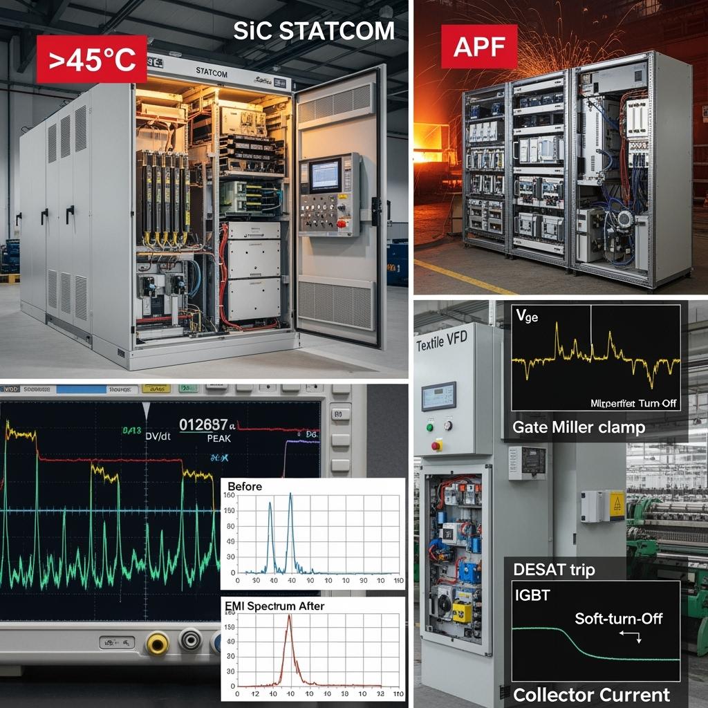
- シンド州風力発電所(複合)のSVG/STATCOM:SiC最適化ドライバにアップグレードすることにより、無効電力ステップ応答が<10 msに改善され、スイッチング損失が約12%削減され、補償チェーン効率が98%を超えました。
- フェイサラバードの繊維VFDフロントエンドレトロフィット:ゲートシェーピングにより、EMIによるトリップが70%削減され、周波数を20 kHzから60 kHzに上げることができ、磁気部品が約25%縮小されました。
- カラチの鉄鋼APF:負のゲートバイアスとミラークランプにより、EAF過渡現象中の誤ったターンオンが排除され、THDがフィルターの再調整を少なくしてIEEE 519の制限内に安定しました。
- KPのセメントプラント補助設備:コンフォーマルコーティングされたゲートドライバアセンブリは、12か月間で<0.5%のドライバ関連の障害イベントで、粉塵シーズンを通じて稼働時間を維持しました。
選択とメンテナンスの考慮事項
- 電気的互換性
- デバイスのゲート電荷と目的のスイッチング速度に合わせてドライバ出力電流(2〜10 Aピーク)を合わせます
- ゲート酸化膜に過度のストレスをかけずにミラーターンオンを抑制するために、負のゲートバイアスレベルを選択します
- UVLOしきい値がMOSFETの要件(+/−レール)に一致していることを確認します
- 絶縁とレイアウト
- MVスタックには強化絶縁を選択し、地域の汚染度に対する沿面距離/空間距離を確認します
- 寄生インダクタンスと測定誤差を最小限に抑えるためのケルビンソースリターンルーティング
- 保護とセンシング
- DESATしきい値設定とブランキング時間は、デバイス特性とトポロジ(NPC/ANPC/MMC)に合わせて調整します
- 熱折り返しのためにダイの近くにNTC/RTDセンシングを組み込みます。メインコントローラへの障害伝搬パスを確保します
- 環境的堅牢性
- 粉塵/湿気の多い場所では、コンフォーマルコーティングとガスケット付きエンクロージャを指定します
- ドライバとゲート抵抗の周囲の空気流または液体冷却パスを検証します
- ライフサイクルとスペア
- ファームウェア/構成のバックアップを維持します。重要なフィーダーの校正済みスペアを保管します
- 運用プロファイルが進化するにつれて、パラメータ調整の年次レビューを計画します
業界の成功要因と顧客の声
- スイッチング周波数、EMIターゲット、およびグリッドコンプライアンスを調整するために、EPC/インテグレータとの早期共同設計
- RG分割、クランプしきい値、およびブランキング時間を最終決定するために、試運転中のオンサイトオシログラフィ
- 診断を解釈し、パラメータの整合性を維持するためのO&Mチームのローカルトレーニング
顧客の声(複合):
「SiC固有のドライバを採用した後、EMIペナルティなしでより高い周波数にプッシュし、グリッドフリッカーイベント中の不要なトリップを排除しました。」—パンジャブ州、繊維クラスター、電気メンテナンス責任者
将来のイノベーションと2025年以降の市場トレンド
- SiCパワーモジュールに統合されたドライバ:より短いループインダクタンス、組み込みセンシング、およびよりスマートな保護
- スイッチング損失を動的に最小限に抑えるための、リアルタイムのデバイス温度と電流を使用した適応ゲート制御
- MMCベースのユーティリティコンバータ向けの高CMTI(>200 kV/µs)および低ジッタのデジタル絶縁
- 重要なインフラストラクチャのIEC 62443に準拠するためのサイバーセキュア診断チャネル
よくある質問と専門家による回答
- 50〜100 kHzのスイッチングでSiCに推奨されるCMTIは何ですか?
≥100〜150 kV/µsが推奨されます。当社の設計は、弱電網およびEAF環境でのマージンのために≥150 kV/µsをターゲットとしています。 - SiC MOSFETに負のゲートバイアスは必要ですか?
特に高速スイッチングまたは高dv/dtトポロジでは、多くの場合はい。ミラークランプ付きの−3〜−5 Vターンオフは、誤ったターンオンのリスクを軽減します。 - DESATとブランキング時間を設定するにはどうすればよいですか?
デバイスSOA、浮遊インダクタンス、およびトポロジに基づいて計算し、FAT/SAT中のオシロスコープキャプチャで検証して、過度のエネルギー散逸なしにソフトターンオフを確保します。 - これらのドライバはIEC 61850システムと統合できますか?
システムレベルでは、メインコントローラはSPI/CAN/光を介してドライバテレメトリを集約し、同期タイムスタンプを使用してIEC 61850 MMS/GOOSEを介して公開します。 - 45°Cを超える動作と粉塵についてはどうですか?
産業グレードのコンポーネント、コンフォーマルコーティング、および熱設計マージンを指定します。エンクロージャは、サイト要件ごとにIP54〜IP65を実現します。
このソリューションがお客様の業務に役立つ理由
高dv/dtおよび温度用に設計されたSiCゲートドライバは、SiC MOSFETの完全な性能(高効率、小型磁気部品、安定したダイナミクス)を解き放ち、障害中のデバイスを保護します。パキスタンの過酷な状況と弱電網の相互接続では、これは直接的にトリップの減少、承認の高速化、および生涯コストの削減につながります。
カスタムソリューションについては専門家にご相談ください
SVG/STATCOM、APF、VFDフロントエンド、およびUPSに最適なゲート駆動戦略を共同設計するために、Sicarb Techと提携してください。
- 10年以上のSiC製造専門知識
- 中国科学院が支援するR&Dと検証
- R‑SiC、SSiC、RBSiC、SiSiC材料およびSiCパワーモジュール全体でのカスタム製品開発
- フィージビリティから試運転まで、技術移転と工場設立サービス
- 材料処理と基板から完成したシステムと制御までのターンキーソリューション
- 測定可能な効率とPQの向上を提供する19以上の企業の実績
無料のコンサルテーション、設計レビュー、およびオンサイト試運転計画を入手してください。
Email: [email protected] | Phone/WhatsApp: +86 133 6536 0038
記事のメタデータ
- 最終更新日:2025年9月11日
- 次回の予定更新日:2025年12月15日
- 作成者:Sicarb Techアプリケーションエンジニアリングチーム
- 参考文献:WBGゲート駆動に関するIEEE Power Electronics Magazine; IEC 62477-1; IEC 60664-1; IEEE 519; IEC 61000-3-6; NTDC/NEPRA相互接続の実践

About the Author: Sicarb Tech
We provide clear and reliable insights into silicon carbide materials, component manufacturing, application technologies, and global market trends. Our content reflects industry expertise, practical experience, and a commitment to helping readers understand the evolving SiC landscape.

Customizable SiC
You May Also Interest
-
![]()
-
![]()
-
![]()
グローバルSiC輸出サービスをシンプルかつ信頼性の高いものに
Global SiC Export Services Made Simple & Reliable In today’s rapidly advancing industrial landscape, the demand for high-performance materials is paramount. Among these, silicon carbide (SiC) stands out as a critical material, essential for pushing the boundaries of various high-temperature, abrasive, and corrosive environments. For engineers, procurement managers, and technical buyers across diverse sectors, sourcing…