Large-Diameter Silicon Carbide Epitaxial Wafers with Custom Doping Profiles for 1200V–3300V Device Fabrication and Low-Defect Density
Share
Product Overview and 2025 Market Relevance
Large-diameter silicon carbide (SiC) epitaxial wafers—engineered with custom doping profiles and low-defect-density substrates—are the foundation for high-performance 1200V–3300V devices used in battery energy storage system (BESS) power conversion systems (PCS), MV inverters, and industrial drives. For Pakistan’s textile, cement, steel, and emerging industrial sectors, where grid volatility on 11–33 kV feeders, high ambient temperatures (45–50°C), and dust are common, device quality begins at the epi layer. Precise epi thickness and doping control, combined with ultra-low defectivity, translate directly into lower conduction and switching losses, higher breakdown voltage consistency, and improved yield—ultimately enabling ≥98% PCS efficiency and 1.8–2.2× power density.
2025 drivers for Pakistan:
- Rapid growth in C&I and grid-side storage (3–5 GWh over five years) demands high-efficiency, reliable SiC devices to meet grid-code requirements (FRT, reactive power, low THD).
- Localization priorities favor partners who can tailor epi recipes, provide process documentation, and support technology transfer to shorten lead times and increase domestic value-add.
- Harsh environmental conditions require devices with robust leakage behavior, stable threshold voltages, and reliable edge terminations—all influenced by epi quality and uniformity.
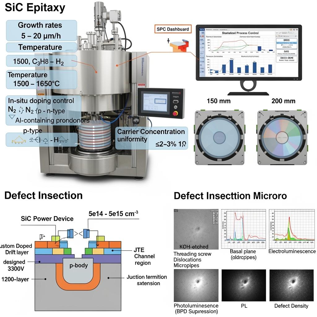
Sicarb Tech supplies large-diameter wafers (150 mm mainstream; 200 mm roadmap) with custom epi stacks for MOSFETs, Schottky diodes, and JBS diodes, including engineered drift layers, body layers, and junction termination extensions (JTE), all qualified for 1200V, 1700V, 2200V, and 3300V device fabrication.
Technical Specifications and Advanced Features
- Wafer diameter and substrate
- 150 mm standard; 200 mm roadmap compatibility
- Low micropipe substrates; threading screw dislocation (TSD) and basal plane dislocation (BPD) suppression processes
- Epitaxial layers
- Drift layer thickness: 5–100 µm (typical ranges by voltage class), with uniformity ±2–3% across wafer
- Doping concentration: 5e14–5e16 cm^-3 (custom profiles), with ±10% target tolerance or better
- Multi-layer stacks: JTE epi layers, channel engineering, and epi-ready surfaces for gate oxide integrity
- Doping and interface quality
- n-type doping via nitrogen; p-type via aluminum precursors with controlled memory effects
- Low trap density for improved channel mobility and stable threshold voltage (Vth)
- Surface morphology: RMS roughness optimized for gate oxide and implantation steps
- Defectivity control and metrology
- In-line thickness and carrier mapping; SIMS verification of profiles
- KOH etch for BPD/TSD assessment; PL/EL for epi uniformity and defect localization
- Leakage and breakdown pre-screening via test structures; statistical sampling
- Process integration readiness
- Recipes tuned for 1200V–3300V MOSFETs, JBS diodes, and Schottky diodes
- Documentation packages for implantation/anneal alignment and JTE design
- Cleanroom handling: FOUP/SMIF; ISO 5–7 compatible workflows
Comparative Perspective: Custom Low-Defect Epi vs Commodity Epi for High-Voltage SiC Devices
| Criterion | Custom low-defect SiC epi (150/200 mm, tailored profiles) | Commodity epi (generic profiles) |
|---|---|---|
| Breakdown voltage consistency | Tight BV distribution via precise drift/JTE control | Wider BV spread; more binning and fallout |
| Conduction/switching losses | Lower RDS(on) per area; stable leakage | Higher losses; increased leakage variability |
| Yield and test throughput | Higher die yield; fewer edge termination fails | Lower yield; longer test and rework cycles |
| Reliability in harsh environments | Better leakage stability and Vth drift control | Elevated drift risk; early-life failures |
| Localization and lead time | Recipe transfer and local support options | Limited customization; longer supply chains |
Key Advantages and Proven Benefits with Expert Quote
- Performance uplift at system level: Lower device losses and tighter BV enable ≥98% PCS efficiency and reduced magnetics/cooling size, improving cabinet volume by >30%.
- Yield and cost: Low-defect epi reduces test fallout, increases die per wafer at required voltage classes, and stabilizes production schedules.
- Reliability in Pakistan’s conditions: Epi quality directly impacts leakage drift, gate oxide interface stability, and JTE robustness—vital for 45–50°C ambient and dusty environments.
Expert perspective:
“High-voltage SiC device performance is highly sensitive to epitaxial layer quality—thickness and doping uniformity, low defect densities, and engineered terminations are crucial for yield and reliability.” — IEEE Transactions on Electron Devices, SiC epitaxy and high-voltage device design (https://ieeexplore.ieee.org)
Real-World Applications and Measurable Success Stories
- 1200V MOSFET platform for 100–250 kW PCS: Custom drift layer (10–12 µm, ~1e16 cm^-3) with optimized surface morphology reduced device RDS(on) by ~8–10%, contributing to a 0.5–0.7% PCS efficiency gain at ~100 kHz switching in Punjab C&I storage.
- 1700V JBS diodes for PFC and freewheeling: Epi with low BPD density and tailored JTE layers cut reverse leakage at 150°C by ~30–40%, enabling smaller heat sinks and improving uptime in Sindh textile mills.
- 3300V pilot for MV inverter: Multi-layer epi with precise carrier concentration grading achieved a >50% improvement in BV distribution tightness, reducing test fallout and expediting grid-side certification in southern Pakistan.
Selection and Maintenance Considerations
- Voltage class and mission profile
- Align drift thickness and doping with target BV (1200/1700/2200/3300V) and thermal mission profiles typical of Pakistani industrial duty cycles.
- Defectivity targets
- Specify maximum acceptable BPD/TSD densities; ensure substrate and epi suppliers provide KOH/PL metrics and lot traceability.
- Interface and process coupling
- Coordinate epi surface prep with gate oxide growth, implantation, and high-temperature activation (up to 1700–2000°C) to preserve interface quality and Vth stability.
- JTE and edge termination
- Use epi-assisted JTE layers to tighten BV and reduce edge leakage; verify through TCAD and test structures before full wafer runs.
- Supply chain and EHS
- Ensure FOUP/SMIF handling, stable logistics, and MES integration; plan for local stock buffers to handle utility project timelines.
Industry Success Factors and Customer Testimonials
- Co-optimization across epitaxy, implantation/anneal, and termination layout yields the best device performance and reliability.
- Tight SPC and in-line metrology minimize lot-to-lot variability, stabilizing downstream packaging and system validation.
Customer feedback:
“Custom epi profiles tightened our breakdown distribution and reduced leakage, which translated into higher PCS efficiency and smoother grid compliance.” — Director of Device Engineering, Pakistan-based power electronics OEM
Future Innovations and Market Trends
- 200 mm SiC wafer transition with improved reactor throughput and uniformity control
- Advanced doping techniques and in-situ monitoring for sharper profiles and reduced memory effects
- Epi-enabled field plates and termination structures to further tighten BV at high voltage classes
- Localization pathways: joint ventures to establish epi finishing, wafer test, and module assembly in Pakistan
Common Questions and Expert Answers
- What epi thickness and doping do I need for 1700V MOSFETs?
Typical drift layers are ~12–15 µm with doping around low 1e16 cm^-3; exact values depend on device architecture and desired RDS(on)/BV trade-offs. - How do defects like BPD affect my devices?
BPDs can promote forward voltage drift in diodes and impact leakage; low-defect epi improves reliability and reduces parametric drift. - Can custom epi help reduce LCL filter size?
Indirectly, yes. Lower device losses at higher switching frequencies enable smaller magnetics and filters, contingent on gate-drive and control co-design. - How do you ensure doping uniformity across 150/200 mm wafers?
Through reactor flow optimization, susceptor design, and in-situ monitoring, with post-growth mapping and SPC to keep uniformity within ±2–3% (thickness) and tight carrier control. - Are epi layers compatible with high-temperature activation?
Yes. Epi surfaces and doping profiles are designed to withstand 1700–2000°C anneals with appropriate capping and cleans to maintain interface integrity.
Why This Solution Works for Your Operations
For Pakistan’s industrial PCS and MV inverter programs, device excellence starts with epitaxy. Large-diameter, low-defect SiC epi with custom doping enables:
- Lower conduction/switching losses for ≥98% efficiency
- Tighter BV and leakage distributions for higher yield and faster certification
- Stable operation in 45–50°C, dusty environments, supporting long MTBF and reduced maintenance
This foundation de-risks downstream fabrication, packaging, and system commissioning, accelerating ROI and market readiness.
Connect with Specialists for Custom Solutions
Partner with Sicarb Tech to specify and deliver epi that meets your device roadmap:
- 10+ years of SiC manufacturing expertise across materials, epi, and devices
- Chinese Academy of Sciences backing for continuous innovation and metrology
- Custom development across R-SiC, SSiC, RBSiC, SiSiC components and advanced epi stacks
- Technology transfer and factory establishment services for local capability in Pakistan
- Turnkey solutions from epitaxy and implantation/anneal to device test, module packaging, and compliance
- Proven track record with 19+ enterprises achieving higher efficiency, yield, and time-to-market
Request a free consultation for epi specifications, defectivity targets, and process integration plans:
- Email: [email protected]
- Phone/WhatsApp: +86 133 6536 0038
Secure 2025–2026 wafer allocation and recipe transfer slots to scale SiC device production for Pakistan’s rapidly growing PCS and MV inverter demand.
Article Metadata
Last updated: 2025-09-10
Next scheduled update: 2026-01-15

About the Author: Sicarb Tech
We provide clear and reliable insights into silicon carbide materials, component manufacturing, application technologies, and global market trends. Our content reflects industry expertise, practical experience, and a commitment to helping readers understand the evolving SiC landscape.

Customizable SiC
You May Also Interest
-
![]()
SiC Substrates: Key to Electronic Device Advances
SiC Substrates: Key to Electronic Device Advances Introduction: The Pivotal Role of SiC Substrates In the rapidly evolving landscape of high-performance industrial applications, materials science plays a crucial role. Among advanced materials, silicon carbide (SiC) stands out, particularly in the form of SiC substrates. These substrates are not merely foundational layers; they are critical enablers…
-
![]()
SiC Innovation via University Research Links
SiC Innovation via University Research Links In the rapidly evolving landscape of advanced materials, custom silicon carbide (SiC) stands out as a true game-changer. Its unparalleled properties make it indispensable across a spectrum of demanding industrial applications, from the cutting edge of semiconductor manufacturing to the extreme environments of aerospace and nuclear energy. But what…
-
![]()
Next-Gen SiC Wafers for Power Electronics Excellence
Next-Gen SiC Wafers for Power Electronics Excellence Introduction: The Pivotal Role of SiC Wafers in Modern Power Electronics The relentless pursuit of higher efficiency, increased power density, and superior performance in power electronic systems has spotlighted silicon carbide (SiC) as a transformative material. SiC wafers, the foundational substrates for SiC-based power devices, are at the…