SiC for More Efficient Power Devices & Systems
Share
SiC for More Efficient Power Devices & Systems
1. Introduction: The SiC Revolution in Power Electronics
The world of power electronics is undergoing a significant transformation, driven by the relentless pursuit of higher efficiency, increased power density, and improved reliability. At the forefront of this revolution is Silicon Carbide (SiC), a wide bandgap semiconductor material poised to displace traditional silicon (Si) in a vast array of demanding applications. Unlike conventional silicon, SiC offers superior material properties that translate directly into tangible performance benefits for power devices and the systems they enable. These advantages include higher breakdown electric field strength, greater thermal conductivity, and a wider bandgap energy. This allows SiC-based power devices to operate at higher voltages, temperatures, and switching frequencies with significantly lower losses.
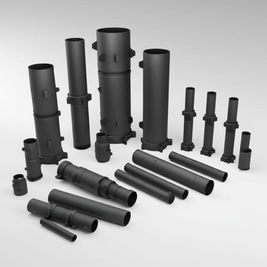
Custom silicon carbide products are becoming increasingly essential as industries from automotive to renewable energy seek to push the boundaries of performance. The ability to tailor SiC components to specific application requirements unlocks new levels of efficiency and innovation. For engineers, procurement managers, and technical buyers, understanding the nuances of SiC technology is crucial for making informed decisions that can lead to competitive advantages and groundbreaking product development. This blog post will delve into the world of SiC for power devices, exploring its applications, benefits, design considerations, and the importance of selecting the right manufacturing partner for your custom SiC needs. As demand for high-performance power semiconductors grows, SiC is no longer a niche material but a cornerstone of next-generation power electronics.
2. Core Applications: Where SiC Power Devices Excel
The exceptional properties of Silicon Carbide have paved the way for its adoption in a diverse range of power electronic applications, particularly where high efficiency, power density, and robust operation are paramount. Industries benefiting from SiC power device integration include:
- Semiconductor Manufacturing: SiC is used not only as the base material for power devices themselves but also in equipment used for semiconductor fabrication, such as wafer handling components and high-temperature process chamber parts, due to its purity and thermal stability.
- Automotive: Electric vehicles (EVs) and hybrid electric vehicles (HEVs) are major drivers for SiC adoption. SiC MOSFETs and diodes are used in main inverters, on-board chargers (OBCs), and DC-DC converters, leading to longer range, faster charging, and reduced vehicle weight.
- Aerospace & Defense: SiC components are ideal for power systems in aircraft, satellites, and defense applications due to their high-temperature tolerance, radiation hardness, and lightweight potential, contributing to more electric aircraft (MEA) initiatives and robust military hardware.
- Power Electronics Manufacturing: This sector broadly utilizes SiC for creating advanced power modules, uninterruptible power supplies (UPS), industrial motor drives, and power factor correction (PFC) circuits. The higher switching frequencies enabled by SiC reduce the size of passive components like inductors and capacitors.
- Renewable Energy: Solar inverters and wind turbine converters benefit significantly from SiC’s efficiency. Higher conversion efficiency means more power harvested from renewable sources, and greater power density allows for smaller and lighter inverter systems.
- Metallurgical Companies: High-temperature induction heating and power supplies for metallurgical processes leverage SiC for its ability to handle extreme conditions and deliver power efficiently.
- Chemical Processing: Power supplies for demanding chemical processes and high-temperature sensors can rely on SiC’s chemical inertness and thermal stability.
- LED Manufacturing: While LEDs themselves are typically GaN-based, the power supplies driving large-scale LED lighting systems can benefit from SiC for improved efficiency and longevity.
- Industrial Machinery & Equipment: Robotics, CNC machines, welding equipment, and various industrial automation systems are incorporating SiC-based motor drives and power supplies for enhanced precision, speed, and energy savings.
- Telecommunications: Power supplies for 5G base stations and data centers are increasingly using SiC to reduce energy consumption and improve thermal management in densely packed environments.
- Oil and Gas: Downhole drilling equipment and power systems in harsh environments benefit from SiC’s ruggedness and high-temperature capabilities.
- Medical Devices: Advanced medical imaging systems (MRI, CT scanners) and specialized medical power supplies can utilize SiC for stable and efficient power delivery.
- Rail Transportation: Traction inverters and auxiliary power supplies in modern trains and trams employ SiC for better energy efficiency, reduced size, and improved reliability.
- Nuclear Energy: Control systems and power conversion in nuclear facilities can benefit from SiC’s radiation tolerance and reliability in critical applications.
The common thread across these diverse applications is the need for power conversion that is more efficient, compact, and reliable, qualities inherently delivered by silicon carbide power electronics.
3. Unlocking Efficiency: Advantages of Custom SiC in Power Systems
The decision to adopt custom Silicon Carbide components in power systems stems from a compelling set of advantages that directly address the core challenges of modern power electronics. These benefits go beyond simple material substitution, enabling system-level improvements:
- Higher Energy Efficiency: SiC devices, such as SiC MOSFETs and SiC Schottky diodes, exhibit significantly lower on-state resistance (RDS(on)) and switching losses compared to their silicon counterparts. This translates to reduced energy waste, less heat generation, and overall higher system efficiency. For applications like EV chargers or solar inverters, this means more power delivered and less energy lost.
- Increased Power Density: Because SiC devices can operate at higher switching frequencies, the size of associated passive components (inductors, capacitors, transformers) can be dramatically reduced. Coupled with lower cooling requirements due to less heat generation, this allows for much more compact and lightweight power electronic systems.
- Superior High-Temperature Performance: Silicon Carbide’s wide bandgap allows it to function reliably at junction temperatures exceeding 200°C, and in some cases, much higher. This is a stark contrast to silicon, which typically has an upper limit around 150-175°C. This resilience opens doors for applications in harsh environments and reduces the complexity of thermal management systems.
- Higher Breakdown Voltage: SiC possesses a breakdown electric field strength approximately ten times that of silicon. This allows for the design of devices that can block much higher voltages in a smaller die area, making it ideal for high-voltage power conversion (e.g., 600V to multi-kV applications).
- Faster Switching Speeds: SiC devices can switch on and off much faster than silicon devices. This capability is crucial for reducing switching losses and enabling the use of higher operating frequencies, which, as mentioned, contributes to smaller system size.
- Improved System Reliability: The inherent robustness of SiC, including its thermal stability and radiation tolerance, contributes to longer operational lifetimes and reduced failure rates in demanding conditions.
- Reduced System Cost (Total Cost of Ownership): While SiC components might have a higher upfront cost compared to silicon in some instances, the system-level benefits often lead to a lower total cost of ownership. Savings can come from reduced cooling needs, smaller passive components, higher efficiency (lower energy consumption), and improved reliability (less maintenance).
- Enhanced Thermal Conductivity: SiC’s thermal conductivity is about three times better than silicon. This allows for more efficient heat dissipation from the device, further contributing to its high-temperature capability and reliability.
Customizing SiC components allows designers to optimize these advantages for their specific application, whether it’s tailoring the die geometry for specific voltage and current ratings or developing unique packaging solutions for extreme thermal or mechanical stress. The ability to fine-tune these parameters through custom SiC solutions is a key enabler for innovation in power electronics.
4. Material Matters: Key SiC Grades for Power Device Performance
Silicon Carbide is a compound semiconductor existing in many different crystal structures called polytypes. For power electronic devices, specific polytypes and material forms are preferred due to their electronic properties. Understanding these distinctions is vital for selecting the optimal SiC material for high-performance applications.
The most commonly used SiC polytypes for power devices are:
- 4H-SiC (Hexagonal Silicon Carbide): This is the dominant polytype for commercial SiC power devices. 4H-SiC offers a superior combination of high electron mobility, high breakdown electric field, and good thermal conductivity. Its properties make it particularly well-suited for high-voltage, high-frequency applications such as MOSFETs and Schottky diodes. The majority of SiC wafers for power electronics are based on the 4H polytype.
- 6H-SiC (Hexagonal Silicon Carbide): While historically significant and still used in some specialized applications (e.g., certain high-frequency devices or high-temperature sensors), 6H-SiC generally has lower electron mobility compared to 4H-SiC, particularly perpendicular to the c-axis. This makes it less favorable for vertical power devices where current flows in that direction. However, it has found use in some RF power devices and LEDs.
- 3C-SiC (Cubic Silicon Carbide): This polytype has the potential advantage of being grown on larger, less expensive silicon substrates. However, 3C-SiC historically suffered from higher defect densities and has not yet achieved the same level of commercial maturity for power devices as 4H-SiC. Research continues, and it may offer cost benefits for specific applications in the future.
Beyond the polytype, SiC materials for power devices are typically processed into these forms:
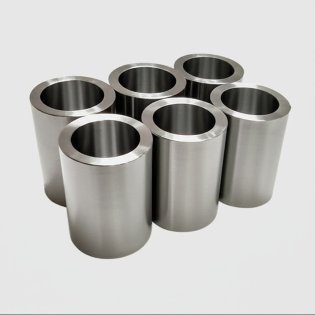
- SiC Substrates (Wafers): These are single-crystal SiC discs, typically ranging from 100mm (4 inches) to 150mm (6 inches) in diameter, with 200mm (8 inches) wafers becoming available. The quality of the substrate, particularly its defect density (e.g., micropipes, basal plane dislocations), is critical for the yield and reliability of the devices fabricated on it. High-quality SiC substrates are fundamental.
- SiC Epitaxial Layers (Epi-layers): A thin, precisely controlled layer of SiC with specific doping concentrations is grown on top of the SiC substrate via epitaxy. This epi-layer is where the active regions of the power device (e.g., the drift region of a MOSFET or diode) are formed. The thickness and doping uniformity of the SiC epitaxy are crucial for device performance, determining characteristics like breakdown voltage and on-resistance.
- Bulk SiC Crystals: While not directly used for planar device fabrication, high-quality bulk SiC crystals are the starting point for producing wafers. The growth techniques, such as Physical Vapor Transport (PVT) or High-Temperature Chemical Vapor Deposition (HTCVD), influence the quality and cost of the final wafers.
The choice of SiC grade and form depends heavily on the intended power device type (e.g., MOSFET, JFET, Schottky diode, PiN diode), its target voltage and current ratings, and the desired operating frequency. Working with a supplier knowledgeable in SiC material science ensures the selection of the most appropriate SiC for optimal device performance and reliability.
5. Designing for Power: Critical Considerations for SiC Devices
Designing power electronic systems with Silicon Carbide devices requires a nuanced approach that leverages SiC’s unique properties while mitigating potential challenges. Engineers must consider several critical aspects to fully realize the benefits of SiC:
- Device Architecture Selection:
- SiC MOSFETs: The most popular choice for new designs due to their voltage-controlled nature, fast switching, and low RDS(on). Planar and trench gate structures each offer different trade-offs in terms of channel mobility, gate charge, and reliability.
- SiC Schottky Diodes (SBDs): Offer near-zero reverse recovery charge, leading to significantly reduced switching losses in circuits where they are used as freewheeling diodes. Often paired with SiC MOSFETs or even silicon IGBTs.
- SiC JFETs: Known for their robustness, JFETs can be normally-on or normally-off. They require specific gate drive strategies but can offer excellent performance in certain applications.
- Other SiC Devices: SiC BJTs (Bipolar Junction Transistors) and Thyristors are also available for very high power applications, though MOSFETs are more common in the medium power ranges.
- Gate Driver Design: SiC MOSFETs, especially, have specific gate drive requirements.
- Voltage Levels: Optimal gate drive voltages (e.g., +20V for turn-on, -2V to -5V for turn-off) are crucial for achieving low RDS(on) and preventing spurious turn-on.
- Speed: Gate drivers must be capable of delivering high peak currents quickly to charge and discharge the gate capacitance rapidly for fast switching.
- Protection: Features like short-circuit protection and desaturation detection are important for device longevity. Miller clamp circuits can prevent parasitic turn-on due to high dv/dt.
- Thermal Management: While SiC operates at higher temperatures, effective heat dissipation is still critical for reliability and performance.
- SiC’s higher thermal conductivity helps spread heat, but careful consideration of die attach, substrate materials, and heatsinking is necessary.
- Advanced cooling techniques like double-sided cooling or liquid cooling might be employed for very high power density applications.
- Layout and Parasitic Inductance/Capacitance Minimization: The fast switching speeds of SiC devices make them sensitive to parasitic inductance and capacitance in the circuit layout.
- Minimizing loop inductances in power paths and gate drive circuits is crucial to reduce voltage overshoots and ringing.
- Careful PCB layout, use of laminated bus bars, and selection of low-inductance packages are important.
- Electromagnetic Interference (EMI) Management: Faster switching transitions (high dv/dt and di/dt) can lead to increased EMI.
- Proper filtering, shielding, and layout techniques are necessary to meet EMI regulations.
- Slowing down switching edges slightly, if permissible by loss targets, can sometimes help manage EMI.
- Device Paralleling: For higher current applications, paralleling SiC devices requires careful attention to ensure current sharing, especially during switching transients. Matching device characteristics and symmetrical layouts are important.
- Reliability and Ruggedness: Understanding failure modes such as gate oxide degradation, body diode degradation (in MOSFETs), and cosmic ray induced failures is important for robust system design. Manufacturers provide data on short-circuit withstand time (SCWT) and avalanche capability.
Effectively addressing these design considerations enables engineers to harness the full potential of custom SiC power solutions, leading to systems that are not only more efficient but also more compact and reliable.
6. Precision Engineering: Tolerances & Finishing for SiC Wafers
The performance and yield of Silicon Carbide power devices are intrinsically linked to the quality and precision of the underlying SiC wafers and epitaxial layers. Manufacturers of SiC substrates and epi-wafers adhere to stringent specifications regarding dimensional accuracy, surface finish, and crystallographic perfection. For procurement managers and technical buyers, understanding these parameters is key to sourcing high-quality materials for device fabrication.
Key parameters for SiC wafers and epi-layers include:
- Diameter and Thickness: Standard diameters include 100mm, 150mm, with 200mm emerging. Thickness is typically specified with tight tolerances (e.g., ±10-25 µm). Consistent thickness is vital for uniform processing in fab lines.
- Total Thickness Variation (TTV): Measures the difference between the maximum and minimum thickness values across the wafer. Low TTV is critical for photolithography and other planar processing steps.
- Bow and Warp: These parameters describe the deviation of the wafer’s median surface from a perfect plane. Excessive bow or warp can cause issues in automated wafer handling and processing equipment.
- Surface Roughness (Ra, Rq, Rz): A smooth, defect-free surface is essential for high-quality epitaxial growth and subsequent device fabrication. Typical surface roughness (Ra) for polished SiC wafers is in the angstrom range (e.g., < 0.5 nm). This is often achieved through Chemical Mechanical Polishing (CMP).
- Subsurface Damage: Grinding and lapping processes used to shape wafers can induce subsurface damage. This damaged layer must be effectively removed by CMP to ensure good epitaxial growth and device performance.
- Flatness (e.g., Site Flatness SFQR): Localized flatness over small areas (sites) where individual dies will be fabricated is critical for fine-line lithography.
- Crystal Orientation: SiC wafers are typically supplied with a specific off-cut angle from the c-axis (e.g., 4° off-axis for 4H-SiC) to promote step-flow growth during epitaxy and reduce certain types of defects. Precise orientation is crucial.
- Defect Density: This is one of the most critical parameters.
- Micropipes (MPD): Hollow tube-like defects that propagate along the c-axis. They are killer defects for power devices. Modern high-quality SiC wafers aim for near zero micropipe density (< 0.1 cm-2).
- Basal Plane Dislocations (BPDs): These defects in the crystal lattice can degrade device performance and reliability, particularly for bipolar devices or the body diode of MOSFETs.
- Threading Screw Dislocations (TSDs) and Threading Edge Dislocations (TEDs): Other types of line defects that can impact device yield and performance.
- Resistivity Uniformity (for conductive substrates): For n-type substrates, uniform resistivity is important for consistent device characteristics.
- Epitaxial Layer Thickness and Doping Uniformity: For epi-wafers, the thickness of the grown layer and its dopant concentration must be extremely uniform across the wafer and from wafer-to-wafer to ensure consistent device parameters like breakdown voltage and RDS(on).
Achieving these tight tolerances and high-quality surface finishes requires sophisticated manufacturing processes, including advanced crystal growth techniques (e.g., PVT), precise slicing and lapping, and multi-step CMP. Suppliers of custom SiC components must demonstrate robust metrology and quality control to ensure their products meet the exacting demands of power device fabrication.
7. From Wafer to Module: Essential Post-Processing for SiC Devices
Once the active SiC device structures are fabricated on the wafer, several crucial post-processing steps are required to transform individual dies into functional and reliable power devices or modules. These steps are critical for ensuring electrical connectivity, mechanical stability, thermal performance, and long-term durability.
Key post-processing stages for SiC power devices include:
- Wafer Backgrinding and Thinning: For vertical power devices, wafers are often thinned from the backside to reduce RDS(on) and improve thermal performance. This process requires careful handling to avoid inducing stress or damage to the thinned wafer.
- Backside Metallization: After thinning, a metal layer (e.g., Ti/Ni/Ag or Ti/Ni/Au) is deposited on the backside of the wafer to form the drain (for MOSFETs) or cathode (for diodes) contact. This layer must provide good ohmic contact and be suitable for die attach.
- Wafer Dicing (Singulation): The processed wafer, containing hundreds or thousands of individual devices, is cut into individual dies. Laser dicing or diamond saw dicing are common methods. Precision is key to avoid chipping or damaging the dies. For SiC, its hardness makes dicing more challenging than for silicon.
- Die Attach: Individual SiC dies are attached to a leadframe, Direct Bonded Copper (DBC) substrate, or other package base. Common die attach materials include solder (e.g., SAC alloys), silver sintering pastes, or epoxy adhesives. The choice depends on thermal performance requirements, operating temperature, and reliability targets. Silver sintering is increasingly popular for SiC due to its high thermal conductivity and reliability at high temperatures.
- Wire Bonding / Interconnects: Electrical connections are made from the top-side contacts (source and gate for MOSFETs, anode for diodes) on the SiC die to the package leads or substrate. Aluminum (Al) or copper (Cu) wires are commonly used. For high-power modules, copper clips or ribbon bonding might be used to reduce inductance and improve current handling.
- Passivation and Encapsulation:
- Passivation: A protective layer (e.g., silicon dioxide, silicon nitride, or polyimide) is often applied to the die surface to protect it from moisture, contamination, and to provide electrical insulation for high-voltage termination structures.
- Encapsulation: The assembled device or module is encapsulated in a molding compound (e.g., epoxy resin) or housed in a hermetic package to provide mechanical protection, environmental sealing, and electrical insulation. The choice of encapsulant is critical for high-voltage SiC devices to prevent partial discharge and ensure long-term reliability.
- Terminal Formation: Leads are formed, plated (e.g., with tin), and trimmed to create the final device terminals for PCB mounting or bus bar connection.
- Testing and Burn-in: Completed devices and modules undergo rigorous electrical testing (static and dynamic parameters), and often burn-in, to screen out early failures and ensure they meet specifications. This includes testing breakdown voltage, leakage currents, on-state resistance, and switching characteristics.
Each of these post-processing steps must be carefully optimized for SiC’s unique material properties, such as its hardness, chemical inertness, and high-temperature operation capability. The success of SiC power modules and discrete devices heavily relies on the quality and precision of these backend manufacturing processes.
8. Overcoming Hurdles: Navigating Challenges in SiC Device Adoption
While Silicon Carbide offers transformative advantages for power electronics, its widespread adoption has faced certain challenges. However, continuous research, development, and manufacturing advancements are progressively addressing these hurdles, making SiC an increasingly viable and compelling option.
Common challenges and their mitigation strategies include:
- Higher Material Cost:
- Challenge: SiC substrates are inherently more expensive to produce than silicon wafers due to the complex, high-temperature crystal growth process and the hardness of the material, which makes slicing and polishing difficult and time-consuming.
- Mitigation:
- Transition to larger diameter wafers (e.g., 150mm to 200mm) helps reduce cost per die.
- Improvements in crystal growth techniques (e.g., faster growth rates, better yield) are lowering substrate costs.
- Increased production volumes lead to economies of scale.
- Focus on Total Cost of Ownership (TCO): While die cost might be higher, system-level savings (smaller passives, reduced cooling, higher efficiency) can offset this.
- Defect Density in Wafers and Epi-layers:
- Challenge: Defects such as micropipes, basal plane dislocations (BPDs), and stacking faults can affect device yield, performance, and long-term reliability. BPDs, for instance, can cause increased leakage current or degradation of the body diode in SiC MOSFETs.
- Mitigation:
- Advanced crystal growth and epitaxy processes are continuously reducing defect densities.
- Improved inspection and metrology techniques allow for better screening of defective material.
- Device designs are being optimized to be more tolerant to certain types of defects.
- Passivation techniques can help mitigate the impact of some surface-related defects.
- Gate Oxide Reliability in SiC MOSFETs:
- Challenge: The interface between the SiC material and the gate dielectric (typically SiO2) in MOSFETs has historically been a concern due to higher interface trap densities compared to Si/SiO2. This can lead to threshold voltage instability and reduced long-term reliability under gate stress.
- Mitigation:
- Advanced gate oxidation processes, such as nitridation (e.g., NO or N2O annealing), have significantly improved the quality and reliability of the SiC/SiO2 interface.
- Development of alternative gate dielectrics is an ongoing research area.
- Device manufacturers implement rigorous screening and qualification tests to ensure gate oxide integrity.
- Short-Circuit Withstand Time (SCWT):
- Challenge: SiC MOSFETs generally have a smaller die size for a given current rating compared to silicon IGBTs. This can lead to a lower thermal mass and potentially shorter SCWT if not properly managed by the gate driver and protection circuitry.
- Mitigation:
- Device designs are optimized to improve SCWT.
- Fast-acting short-circuit detection and protection mechanisms in the gate driver are crucial.
- Some manufacturers offer SiC MOSFETs with enhanced SCWT ratings.
- Dynamic RDS(on) Increase:
- Challenge: Some SiC MOSFETs can exhibit an increase in on-state resistance after being subjected to high-voltage blocking conditions, due to charge trapping phenomena.
- Mitigation: Advances in material quality (especially substrate and epitaxy) and device processing have greatly reduced this effect in modern SiC MOSFETs.
- Manufacturing Complexity:
- Challenge: Processing SiC is more complex than silicon due to its hardness, chemical inertness, and the need for very high temperatures in processes like ion implantation annealing.
- Mitigation: Development of specialized SiC processing equipment and refinement of process recipes are ongoing. Investment in dedicated SiC fabs is increasing.
By understanding these challenges and the ongoing efforts to overcome them, engineers and procurement professionals can make more informed decisions when incorporating SiC technology into their products. Collaborating with experienced SiC suppliers who are at the forefront of these advancements is key.
9. Partnering for Success: Choosing Your SiC Component Supplier
Selecting the right supplier for your custom Silicon Carbide components is a critical decision that can significantly impact your product’s performance, reliability, time-to-market, and overall cost-effectiveness. Given the specialized nature of SiC manufacturing, a prospective partner should be evaluated on several key criteria:
- Technical Expertise and Experience:
- Look for suppliers with deep knowledge of SiC material science, device physics, and manufacturing processes specific to SiC (crystal growth, epitaxy, wafer fabrication, device design, post-processing).
- Experience with your specific application area (e.g., automotive,

About the Author: Sicarb Tech
We provide clear and reliable insights into silicon carbide materials, component manufacturing, application technologies, and global market trends. Our content reflects industry expertise, practical experience, and a commitment to helping readers understand the evolving SiC landscape.

Customizable SiC
You May Also Interest
-
![]()
Key SiC Exporters in Asia for International Trade
Key SiC Exporters in Asia for International Trade In the rapidly evolving landscape of advanced materials, silicon carbide (SiC) stands out as a material of unparalleled performance. Its exceptional properties make it indispensable across a spectrum of demanding industrial applications. For businesses seeking reliable and high-quality silicon carbide products, understanding the key players and regions…
-
![]()
SiC Substrates: Key to Electronic Device Advances
SiC Substrates: Key to Electronic Device Advances Introduction: The Pivotal Role of SiC Substrates In the rapidly evolving landscape of high-performance industrial applications, materials science plays a crucial role. Among advanced materials, silicon carbide (SiC) stands out, particularly in the form of SiC substrates. These substrates are not merely foundational layers; they are critical enablers…
-
![]()
SiC Innovation via University Research Links
SiC Innovation via University Research Links In the rapidly evolving landscape of advanced materials, custom silicon carbide (SiC) stands out as a true game-changer. Its unparalleled properties make it indispensable across a spectrum of demanding industrial applications, from the cutting edge of semiconductor manufacturing to the extreme environments of aerospace and nuclear energy. But what…