SiC Enhancing RF Device Performance & Reliability
Share
SiC Enhancing RF Device Performance & Reliability
Introduction: The Unseen Powerhouse – Custom SiC in RF Technology
In the rapidly evolving landscape of radio frequency (RF) technology, the demand for higher performance, greater reliability, and more compact solutions is relentless. From advanced telecommunications systems and radar technology to cutting-edge medical devices and industrial heating, RF devices are pivotal. At the heart of this progression lies a remarkable material: Silicon Carbide (SiC). Custom silicon carbide products are becoming increasingly essential in high-performance RF applications, offering a unique combination of properties that push the boundaries of what’s possible. This blog post will delve into how SiC is revolutionizing RF device performance and reliability, exploring its applications, advantages, design considerations, and how to select the right manufacturing partner for your critical needs. For engineers, procurement managers, and technical buyers in industries like semiconductors, aerospace, and power electronics, understanding the nuances of custom SiC is key to unlocking next-generation RF capabilities.
The integration of custom SiC components into RF systems is not just an upgrade; it’s a transformative step. Traditional materials like silicon (Si) and gallium arsenide (GaAs) have served the RF industry well, but they are increasingly hitting their operational limits, especially at high power densities, high frequencies, and extreme temperatures. Silicon Carbide, a wide-bandgap semiconductor, emerges as a superior alternative, enabling RF devices to operate more efficiently and reliably under demanding conditions. This makes technical ceramics like SiC indispensable for next-generation RF infrastructure, from 5G base stations to sophisticated military radar systems and satellite communications.
The Critical Impact of SiC on Modern RF Device Capabilities
Silicon Carbide’s influence on modern RF devices is profound, directly addressing the core challenges of power, frequency, and thermal management. Its exceptional material properties translate into tangible performance gains across a spectrum of RF applications. For instance, SiC RF power transistors and amplifiers can handle significantly higher power levels and operate at higher temperatures than their silicon-based counterparts. This leads to smaller, more efficient power modules, reducing system size and cooling requirements – a critical factor in aerospace, defense, and portable communication devices.
Furthermore, the high breakdown electric field of SiC (approximately 10 times that of silicon) allows for the fabrication of devices that can withstand much higher voltages. This is particularly beneficial for high-power RF applications such as broadcast transmitters and industrial plasma generation. The material’s high saturated electron velocity also contributes to its suitability for high-frequency operation, enabling clearer signals and greater bandwidth in telecommunications and radar systems. The use of high-frequency SiC substrates is also instrumental in developing compact and efficient passive RF components like filters and couplers, further underscoring SiC’s versatility and importance in the RF domain. Industries from automotive radar systems to renewable energy inverters requiring robust RF communication are increasingly turning to silicon carbide RF packaging solutions for enhanced durability.
Why Custom Silicon Carbide is a Game-Changer for RF Applications
The decision to opt for custom silicon carbide in RF applications stems from its unparalleled combination of electrical, thermal, and mechanical properties, which collectively address the stringent demands of modern RF systems. Generic, off-the-shelf components often fall short when specific performance metrics, form factors, or operational environments are critical. Customization allows engineers to leverage SiC’s inherent advantages precisely where they are needed most.
- Superior Thermal Management: SiC boasts a thermal conductivity roughly three times higher than silicon and significantly better than many other semiconductor materials. This allows RF devices to dissipate heat more effectively, leading to lower operating temperatures, improved performance stability, and enhanced reliability. For high-power RF amplifiers and transmitters, this means less reliance on bulky and complex cooling systems.
- Enhanced Power Handling: With a high critical electric field strength (around 2.5-3 MV/cm), SiC devices can handle significantly higher voltages and power densities compared to Si or GaAs. This translates to more powerful RF signals from smaller device footprints, crucial for applications like radar, electronic warfare, and 5G/6G base stations.
- Higher Frequency Operation: SiC’s high electron saturation velocity allows for faster switching speeds, enabling operation at higher frequencies. This is essential for advanced communication systems, satellite links, and high-resolution radar, pushing the boundaries of data transmission and detection.
- Increased Reliability and Lifespan: The inherent robustness of SiC, including its resistance to high temperatures and radiation, contributes to longer operational lifespans and greater reliability of RF devices, even in harsh environments encountered in aerospace, defense, and industrial settings. This reduces maintenance costs and improves system uptime.
- Reduced Size, Weight, and Power (SWaP): The ability of SiC to handle more power in smaller packages and operate efficiently at higher temperatures allows for a significant reduction in the overall size, weight, and power consumption of RF systems. This is a critical advantage in mobile, airborne, and space-based applications.
- Tailored Performance: Customization allows for the optimization of SiC material properties (e.g., doping levels, crystal orientation) and component design (e.g., geometry, metallization) to meet specific RF performance targets, such as maximizing gain, minimizing noise figure, or achieving specific impedance matching.
By choosing custom SiC RF solutions, companies can gain a competitive edge, developing RF systems that are more powerful, efficient, compact, and reliable than ever before. This tailored approach ensures that the final component integrates seamlessly and performs optimally within the larger RF system.
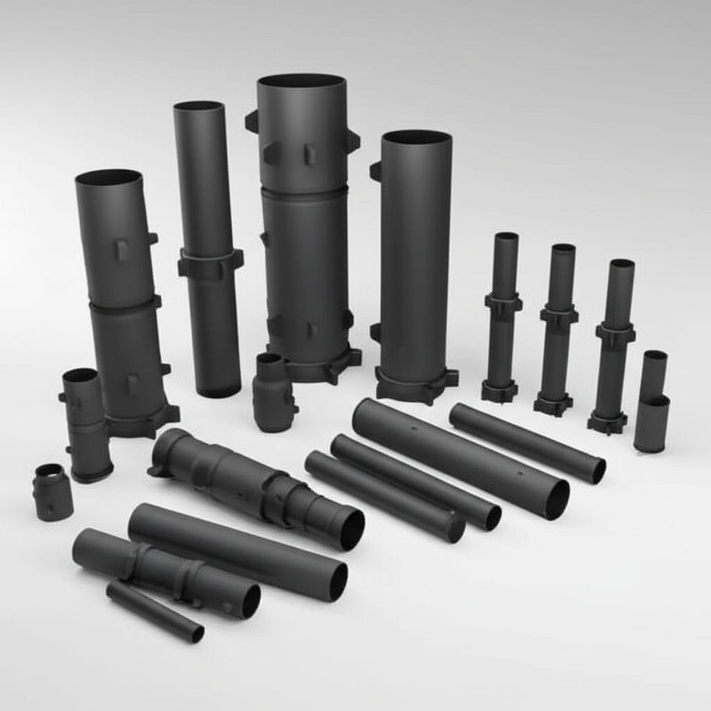
Key Silicon Carbide Grades and Compositions for Optimal RF Performance
The performance of SiC-based RF devices is heavily dependent on the specific grade and polytype of the silicon carbide material used. Different applications within the RF spectrum have varying requirements for electrical conductivity, resistivity, and crystal quality. Understanding these nuances is critical for selecting the appropriate SiC for your custom component.
| SiC Grade/Type | Key Characteristics for RF | Common RF Applications |
|---|---|---|
| High-Purity Semi-Insulating (HPSI) 4H-SiC | Very high resistivity (>109 Ω·cm), low RF losses, good thermal conductivity, high breakdown field. Essential for minimizing substrate-induced losses and ensuring signal integrity at high frequencies. | Substrates for Gallium Nitride (GaN) High Electron Mobility Transistors (HEMTs) used in RF power amplifiers, Monolithic Microwave Integrated Circuits (MMICs), RF switches, and passive components. |
| Conductive n-type 4H-SiC | Controlled doping levels (typically nitrogen) for specific conductivity, high electron mobility, excellent thermal conductivity. Used for active device layers. | RF power MOSFETs, Schottky diodes (though less common for primary RF amplification, more for power conditioning within RF systems), and as conductive buffer layers in GaN-on-SiC structures. |
| Vanadium-doped Semi-Insulating SiC | Historically used for achieving semi-insulating properties. Vanadium acts as a deep-level dopant, compensating residual shallow donors or acceptors. | Older generation SiC substrates for RF devices. Largely superseded by HPSI SiC due to concerns about vanadium diffusion and trapping effects impacting device performance and reliability. |
| Polycrystalline SiC | Lower cost, good thermal conductivity, and mechanical strength. Not typically used for active RF device layers due to grain boundaries affecting electronic properties but can be considered for thermal management components or packaging. | Heat spreaders, structural supports in RF modules, and some types of RF absorbers or shielding where high electrical resistivity is not the primary concern. |
The 4H polytype of SiC (4H-SiC) is predominantly favored for RF and power electronics applications due to its superior electronic properties, including higher electron mobility and a wider bandgap compared to other polytypes like 6H-SiC. For RF applications, especially in GaN-on-SiC technology, the quality of the semi-insulating SiC substrate is paramount. It must exhibit extremely low levels of impurities and defects to ensure high resistivity, low dielectric losses, and a stable platform for the epitaxial growth of GaN layers. The choice of SiC material directly impacts the final device’s gain, efficiency, linearity, and overall reliability, making collaboration with knowledgeable silicon carbide manufacturers crucial for optimizing RF component performance.
Strategic Design Considerations for Custom SiC RF Components
Designing custom SiC RF components requires a meticulous approach that balances electrical performance with thermal management, manufacturability, and reliability. The unique properties of silicon carbide offer tremendous potential, but harnessing this potential effectively means paying close attention to specific design rules and considerations that may differ significantly from those for traditional semiconductor materials.
Key Design Parameters for SiC RF Devices:
- Operating Frequency and Bandwidth: The target frequency range will influence material selection (specifically the quality of semi-insulating SiC), device geometry, and packaging. Higher frequencies demand tighter tolerances and minimized parasitic capacitances and inductances.
- Power Levels (Input/Output): Expected power handling capability dictates the active device area, thermal design, and metallization schemes. SiC’s high power density capabilities allow for smaller device sizes, but efficient heat extraction remains critical.
- Thermal Management Strategy: Despite SiC’s excellent thermal conductivity, high-power RF devices generate significant heat. Design considerations must include pathways for efficient heat dissipation. This involves optimizing the die attach, choice of heat sink materials, and potentially incorporating advanced cooling techniques. The thermal expansion coefficient mismatch between SiC and packaging materials also needs careful management.
- Impedance Matching: Achieving proper impedance matching (typically to 50 Ohms) is vital for efficient power transfer and minimizing signal reflections. This involves careful layout of transmission lines, matching networks, and consideration of SiC’s dielectric properties.
- Device Geometry and Layout: The physical layout of transistors, inductors, capacitors, and interconnects on the SiC substrate must be optimized to minimize losses, reduce crosstalk, and manage electric field distributions to prevent premature breakdown. Aspects like gate length, source-drain spacing, and via placement are critical.
- Parasitic Effects: At high RF frequencies, parasitic capacitances and inductances associated with bond wires, package leads, and on-chip structures can severely degrade performance. Design simulations must accurately model these parasitics to mitigate their impact.
- Material Purity and Defect Density: For optimal RF performance, particularly for low-noise amplifiers or high-linearity devices, the SiC substrate must have high purity and low crystallographic defect density. These factors are primarily material supplier-dependent but influence design rules.
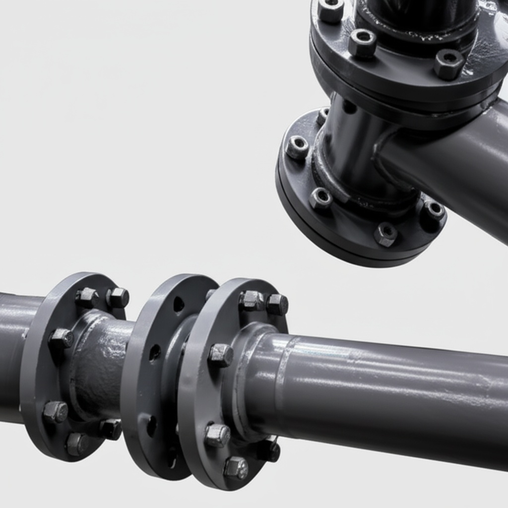
- Packaging and Interconnects: The choice of packaging technology (e.g., surface mount, flange mount, chip-on-board) and interconnects (e.g., wire bonds, flip-chip) must be compatible with SiC’s high operating temperatures and the RF performance requirements. Hermetic sealing may be necessary for reliability in harsh environments.
- Manufacturability and Cost: While pushing performance boundaries, designs must also consider the practical aspects of fabrication, including achievable tolerances, processing yields, and overall cost. Complex designs can lead to higher manufacturing costs and longer lead times.
Effective design of custom SiC RF components often involves sophisticated simulation tools (e.g., electromagnetic and thermal modeling software) to predict device behavior and optimize the design before fabrication. Collaboration between the RF design engineers and the SiC material/foundry experts is crucial to navigate these considerations successfully, leading to robust and high-performing RF devices.
Achieving Precision: Tolerance, Surface Finish, and Dimensional Accuracy in SiC RF Parts
The performance of Silicon Carbide RF components at high frequencies is critically dependent on the precision achieved during manufacturing. Tight tolerances, superior surface finishes, and high dimensional accuracy are not just desirable but essential for ensuring consistent device performance, minimizing signal loss, and maintaining signal integrity. These factors directly influence parasitic capacitances, impedance matching, and the overall reliability of the RF module.
Achievable tolerances for custom silicon carbide components vary depending on the manufacturing process (e.g., wafer dicing, grinding, lapping, polishing) and the complexity of the part. Typical dimensional tolerances can range from tens of microns down to a few microns for critical features. For instance:
- Thickness Uniformity: For SiC wafers used as substrates, thickness uniformity across the entire wafer is crucial for consistent epitaxial growth (e.g., GaN on SiC) and subsequent device processing. Variations can lead to inconsistencies in device characteristics.
- Flatness and Bow: Substrate flatness (Total Thickness Variation, TTV) and bow affect photolithography processes and can induce stress in overlying epitaxial layers. Strict control is necessary.
- Lateral Dimensions: The precision of dicing or etching processes determines the final dimensions of individual chips or discrete components. This is critical for fitment within packages and for defining features like transmission lines or capacitor areas.
Surface finish is another paramount consideration for RF applications. A smooth surface with minimal subsurface damage is vital for several reasons:
- Reduced RF Losses: Surface roughness can increase conductor losses at high frequencies due to the skin effect, where current concentrates near the surface. A smoother surface leads to lower signal attenuation.
- Improved Epitaxial Growth: For GaN-on-SiC devices, the surface quality of the SiC substrate directly impacts the quality of the GaN epitaxial layer. A pristine, defect-free surface is required for achieving high electron mobility and low defect density in the GaN channel. Chemical Mechanical Polishing (CMP) is often employed to achieve angstrom-level surface roughness (Ra < 0.5 nm).
- Enhanced Metallization Adhesion: A clean and smooth surface promotes better adhesion of metal contacts and interconnects, improving reliability and reducing contact resistance.
Dimensional accuracy across all features of the SiC component ensures that the fabricated device behaves as predicted by design simulations. Deviations can lead to shifts in resonant frequencies, impedance mismatches, and degraded overall performance. Therefore, sophisticated metrology techniques, including atomic force microscopy (AFM) for surface roughness, X-ray diffraction (XRD) for crystal quality, and advanced optical inspection systems for dimensional control, are integral to the manufacturing of high-quality SiC RF parts. Partnering with a supplier who demonstrates rigorous process control and metrology capabilities is key to obtaining SiC components that meet the exacting demands of RF applications.
Essential Post-Processing Techniques for SiC RF Device Optimization
Once the basic silicon carbide RF device structure is fabricated, several post-processing steps are often necessary to optimize its performance, enhance its durability, and prepare it for integration into larger systems. These techniques are tailored to address specific RF requirements and the inherent properties of SiC. Careful execution of these steps is critical for realizing the full potential of custom SiC RF components.
Common Post-Processing Steps:
- Backside Grinding/Thinning: SiC wafers are often thinned after front-side processing to reduce thermal resistance, improve heat dissipation, and meet specific package height requirements. This is particularly important for high-power RF devices where efficient thermal management is paramount. Precision grinding is followed by stress relief processes to prevent wafer breakage.
- Metallization: Creating low-resistance ohmic contacts and robust Schottky contacts is crucial for RF device performance. This involves depositing specific metal stacks (e.g., Ti/Pt/Au, Ni/Au) followed by annealing at high temperatures. The choice of metals and annealing conditions is optimized for the type of SiC (n-type or p-type) and the specific application (e.g., gates, drains, sources, pads). Metallization also includes the formation of interconnects and transmission lines.
- Passivation: A dielectric layer (e.g., SiO2, Si3N4) is typically deposited to protect the SiC surface, reduce surface leakage currents, and provide electrical isolation between components. The quality of the passivation layer and its interface with SiC can significantly impact device stability and reliability, especially at high voltages and temperatures.
- Dicing and Die Separation: Wafers containing multiple RF devices are diced into individual chips. Laser dicing or diamond saw cutting are common methods. The dicing process must be carefully controlled to minimize chipping and mechanical stress, which could compromise device integrity.
- Surface Treatments/Coatings: In some cases, specialized surface treatments or coatings may be applied to enhance certain properties. For example, anti-reflective coatings for optoelectronic aspects or protective coatings for harsh environments. For RF applications, specific surface functionalization might be used to improve bonding or encapsulation.
- Via Hole Formation: Through-wafer vias (TWVs) are often created in SiC substrates, especially for GaN-on-SiC MMICs. These vias provide low-inductance ground connections, improve RF performance, and aid in thermal management. Reactive Ion Etching (RIE) is a common technique for creating these vias.
- Testing and Burn-in: Before final assembly, individual SiC RF devices undergo rigorous electrical testing (DC and RF) to ensure they meet specifications. Burn-in testing at elevated temperatures and voltages may also be performed to screen out early failures and improve overall product reliability.
Each of these post-processing steps requires specialized equipment and expertise. The complexity and sequence of these steps depend heavily on the specific RF device being manufactured (e.g., transistor, MMIC, passive component) and its intended application. Effective post-processing is a hallmark of high-quality silicon carbide RF packaging and component manufacturing, ensuring that the devices deliver optimal performance and long-term reliability in demanding RF systems.
Overcoming Common Hurdles in SiC RF Component Manufacturing
While silicon carbide offers significant advantages for RF applications, its manufacturing presents unique challenges that must be adeptly managed. The material’s extreme hardness, chemical inertness, and tendency towards certain crystallographic defects require specialized knowledge, advanced equipment, and stringent process controls. Overcoming these hurdles is key to producing high-quality, reliable SiC RF devices at a competitive cost.
Key Manufacturing Challenges and Mitigation Strategies:
- Material Quality and Defect Control:
- Challenge: SiC crystal growth (boule production) can result in defects such as micropipes, dislocations, and stacking faults, which can impair device performance and reliability. Achieving large-diameter, high-purity, low-defect semi-insulating substrates is particularly challenging.
- Mitigation: Advanced crystal growth techniques (e.g., High-Temperature Chemical Vapor Deposition – HTCVD, Physical Vapor Transport – PVT) with precise control over temperature, pressure, and source materials. Rigorous material characterization and screening to select wafers with acceptable defect densities. Continuous R&D in boule growth and wafering processes.
- Wafer Processing and Machining:
- Challenge: SiC’s hardness (Mohs hardness of 9.0-9.5) makes sawing, grinding, lapping, and polishing difficult and time-consuming, leading to higher tool wear and processing costs. It can also induce subsurface damage if not done correctly.
- Mitigation: Use of diamond-based abrasives and specialized machinery. Optimization of machining parameters (e.g., speed, feed rate, coolant). Advanced polishing techniques like Chemical Mechanical Polishing (CMP) to achieve ultra-smooth, damage-free surfaces. Laser machining can be an alternative for certain applications.
- Doping and Ion Implantation:
- Challenge: Achieving precise and uniform doping profiles in SiC through ion implantation is difficult due to its density. Post-implantation annealing required for dopant activation needs very high temperatures (often >1700°C), which can damage the SiC surface or lead to dopant redistribution if not carefully controlled.
- Mitigation: Optimized implantation energies and doses. Development of advanced annealing techniques (e.g., microwave annealing, laser annealing) and protective capping layers during annealing to preserve surface integrity. Careful characterization of doping profiles.
- Etching:
- Challenge: SiC’s chemical inertness makes wet etching very slow and impractical for fine feature definition. Dry etching processes (e.g., RIE, Inductively Coupled Plasma – ICP etching) are used but can be complex to optimize for selectivity, etch rate, and anisotropy.
- Mitigation: Development of specific plasma chemistries (fluorine-based gases like SF6, CHF3) and etching process parameters. Use of robust etch masks. Careful endpoint detection to control etch depth.
- Ohmic Contact Formation:
- Challenge: Forming low-resistance, thermally stable ohmic contacts to both n-type and p-type SiC is challenging, especially for p-type SiC due to its wide bandgap and the difficulty in finding metals with suitable work functions. High annealing temperatures are typically required.
- Mitigation: Research into optimal metal schemes (e.g., Ti/Al for n-type, Ni/Ti/Al for p-type) and surface preparation techniques. Precise control over annealing conditions (temperature, time, atmosphere) to achieve low contact resistivity and good morphology.
- Thermal Management in Devices:
- Challenge: While SiC has high thermal conductivity, the extreme power densities in some RF devices still necessitate sophisticated thermal management solutions to prevent overheating and ensure reliability.
- Mitigation: Advanced device design to spread heat, use of thinned substrates, high-conductivity die-attach materials, and efficient heat sinking. Integration of microfluidic cooling or diamond heat spreaders in extreme cases.
- Cost of Manufacturing:
- Challenge: The complexities mentioned above, coupled with relatively lower production volumes compared to silicon, contribute to higher manufacturing costs for SiC devices.
- Mitigation: Continuous process improvements, development of larger diameter wafers (e.g., 150mm and 200mm), higher yielding processes, and economies of scale as adoption increases. Strategic partnerships with experienced suppliers offering competitive solutions.
Addressing these challenges requires a deep understanding of materials science, semiconductor physics, and manufacturing engineering. Companies specializing in custom silicon carbide manufacturing invest heavily in R&D and process technology to mitigate these issues and deliver high-performance RF components reliably.
Selecting Your Ideal Partner: Choosing a Custom SiC RF Component Supplier
The success of your RF project hinges significantly on the capabilities and reliability of your custom silicon carbide component supplier. Choosing the right partner is a strategic decision that goes beyond just cost. It involves evaluating technical expertise, manufacturing prowess, quality assurance systems, and the ability to collaborate effectively to meet specific and often demanding RF application requirements. For procurement managers and technical buyers, identifying a supplier who can act as a long-term partner is crucial for sustained innovation and supply chain stability.
Key Criteria for Evaluating SiC Suppliers:
- Technical Expertise and Experience: Does the supplier have a deep understanding of SiC materials science, RF device physics, and the specific challenges of SiC processing for RF applications? Look for a proven track record, experienced engineering teams, and relevant case studies or examples of past work.
- Material Quality and Sourcing: Enquire about the source and quality of their SiC substrates. Do they have control over or strong partnerships for sourcing high-purity, low-defect semi-insulating SiC tailored for RF? Material consistency is paramount.
- Customization Capabilities: Can the supplier genuinely offer custom solutions? This includes custom design, material property adjustments (within limits), specific dimensional tolerances, unique surface finishes, and tailored post-processing. Assess their flexibility and willingness to engage in co-development. Our customizing support ensures we can meet diverse and specific client needs effectively.
- Manufacturing Facilities and Processes: Evaluate their manufacturing infrastructure. Do they possess advanced equipment for SiC growth (if applicable), wafering, epitaxy (if offering GaN-on-SiC), lithography, etching, metallization, and testing? Are their processes well-documented and controlled?
- Quality Management Systems: Look for certifications like ISO 9001. What quality control measures are in place at each stage of production? How do they handle material traceability, process monitoring, and final product testing?
- Metrology and Characterization Capabilities: A supplier’s ability to measure and verify critical parameters (e.g., resistivity, defect density, surface roughness, dimensional accuracy, RF performance) is essential. Advanced metrology tools demonstrate a commitment to quality.
- Lead Times and Scalability: Can the supplier meet your prototype and volume production timelines? Do they have the capacity to scale up production if your demand grows? Transparent communication regarding lead times is crucial.
- Cost-Effectiveness: While not the sole factor, pricing must be competitive. Understand the cost structure and ensure you are receiving good value for the level of quality and customization offered.
- Technical Support and Communication: Effective and responsive communication is vital, especially for custom projects. Does the supplier offer strong technical support throughout the design, manufacturing, and post-delivery phases?
- Location and Supply Chain Resilience: Consider the supplier’s location and its implications for logistics and supply chain risk. Some regions have become significant hubs for SiC manufacturing. For instance, the hub of China’s silicon carbide customizable parts manufacturing is situated in Weifang City. This region is home to over 40 SiC production enterprises, collectively accounting for more than 80% of China’s total SiC output.
Companies like Sicarb Tech have been instrumental in the development of such hubs. Since 2015, SicSino has been introducing and implementing advanced silicon carbide production technology, assisting local enterprises in Weifang to achieve large-scale production and technological breakthroughs. As part of the Chinese Academy of Sciences (Weifang) Innovation Park, an entrepreneurial park collaborating closely with the National Technology Transfer Center of the Chinese Academy of Sciences , SicSino leverages the formidable scientific, technological capabilities, and talent pool of Chinese Academy of Sciences. This backing ensures a reliab

About the Author: Sicarb Tech
We provide clear and reliable insights into silicon carbide materials, component manufacturing, application technologies, and global market trends. Our content reflects industry expertise, practical experience, and a commitment to helping readers understand the evolving SiC landscape.

Customizable SiC
You May Also Interest
-
![]()
Key SiC Exporters in Asia for International Trade
Key SiC Exporters in Asia for International Trade In the rapidly evolving landscape of advanced materials, silicon carbide (SiC) stands out as a material of unparalleled performance. Its exceptional properties make it indispensable across a spectrum of demanding industrial applications. For businesses seeking reliable and high-quality silicon carbide products, understanding the key players and regions…
-
![]()
SiC Substrates: Key to Electronic Device Advances
SiC Substrates: Key to Electronic Device Advances Introduction: The Pivotal Role of SiC Substrates In the rapidly evolving landscape of high-performance industrial applications, materials science plays a crucial role. Among advanced materials, silicon carbide (SiC) stands out, particularly in the form of SiC substrates. These substrates are not merely foundational layers; they are critical enablers…
-
![]()
SiC Innovation via University Research Links
SiC Innovation via University Research Links In the rapidly evolving landscape of advanced materials, custom silicon carbide (SiC) stands out as a true game-changer. Its unparalleled properties make it indispensable across a spectrum of demanding industrial applications, from the cutting edge of semiconductor manufacturing to the extreme environments of aerospace and nuclear energy. But what…