Semiconductor Evolution Fueled by SiC Technology
Share
Semiconductor Evolution Fueled by SiC Technology
The semiconductor industry is in a constant state of evolution, driven by the relentless demand for smaller, faster, and more efficient electronic devices. As traditional silicon-based technologies approach their theoretical limits, new materials are emerging to push the boundaries of performance. Among these, Silicon Carbide (SiC) has distinguished itself as a transformative material, particularly for high-power, high-frequency, and high-temperature applications. This blog post explores the pivotal role of SiC in the ongoing semiconductor evolution, delving into its advantages, applications, and the considerations for sourcing custom SiC components.
The Semiconductor Landscape in Transformation
For decades, silicon (Si) has been the undisputed workhorse of the semiconductor industry. However, the increasing power densities, operating frequencies, and harsh environmental conditions in modern applications—from electric vehicles to 5G infrastructure and renewable energy systems—are exposing the limitations of silicon. Parameters such as breakdown voltage, thermal conductivity, and electron mobility in silicon are being stretched to their feasible maximums. This is where wide-bandgap (WBG) semiconductors, prominently Silicon Carbide, enter the scene. SiC offers superior material properties that directly translate into significant performance improvements in semiconductor devices, heralding a new era of power electronics and advanced semiconductor systems. The shift towards SiC is not merely an incremental upgrade; it’s a foundational change enabling entirely new capabilities and efficiencies across numerous industries.
Why SiC is a Game-Changer for Semiconductors
Silicon Carbide’s prominence in the semiconductor industry isn’t accidental; it’s a direct result of its exceptional material properties that allow for device performance far exceeding that of conventional silicon. These advantages are critical for engineers and designers looking to create next-generation power electronics and high-performance systems.
- Higher Breakdown Electric Field: SiC possesses a breakdown electric field approximately ten times higher than that of silicon. This allows SiC devices to block significantly higher voltages in a much thinner layer, leading to smaller device sizes and lower on-state resistance for a given voltage rating. This is crucial for high-voltage power conversion and distribution.
- Superior Thermal Conductivity: SiC exhibits thermal conductivity about three times better than silicon. This enables SiC devices to dissipate heat more effectively, allowing them to operate at higher temperatures and power densities without requiring bulky cooling systems. This property enhances reliability and reduces system size and cost.
- Wider Bandgap: SiC has a bandgap roughly three times wider than silicon (e.g., ~3.2 eV for 4H-SiC vs. 1.1 eV for Si). This wider bandgap results in lower leakage currents, especially at elevated temperatures, and allows for higher operating temperatures – often exceeding 200°C, compared to silicon’s typical limit of 150°C.
- Higher Electron Saturated Drift Velocity: SiC supports a saturated electron drift velocity about twice that of silicon. This characteristic enables SiC devices to operate at higher switching frequencies, leading to smaller passive components (inductors, capacitors) in power converter systems, thereby increasing power density and reducing system volume.
- Enhanced Radiation Hardness: The strong atomic bonds in SiC make it inherently more resistant to radiation damage compared to silicon. This makes SiC devices highly suitable for aerospace, defense, and nuclear energy applications where radiation tolerance is a critical requirement.
These intrinsic benefits mean SiC devices can be smaller, faster, more efficient, and more reliable than their silicon counterparts, particularly in demanding applications. This translates to tangible advantages for procurement managers and technical buyers, including reduced system costs, improved energy efficiency, and enhanced product longevity.
Key SiC Applications in the Semiconductor Ecosystem
The superior properties of Silicon Carbide have unlocked a diverse range of applications within the semiconductor industry, driving innovation and efficiency improvements. As engineers and procurement specialists evaluate materials, understanding these specific use cases highlights SiC’s value proposition.
SiC technology is enabling breakthroughs in several key areas:
- Power Electronics: This is arguably the most significant area for SiC.
- Inverters and Converters: Used in electric vehicles (EVs) for traction inverters, on-board chargers (OBCs), and DC-DC converters. SiC enables higher efficiency, leading to longer EV range and faster charging. Solar inverters and wind turbine converters also benefit from SiC’s efficiency and power density.
- Power Supplies: Industrial power supplies, server farm PSUs, and telecommunications rectifiers leverage SiC for reduced energy consumption and smaller form factors.
- Motor Drives: SiC-based variable frequency drives (VFDs) for industrial motors offer better control and energy savings.
- Radio Frequency (RF) Devices:
- Radar Systems: SiC’s high power density and thermal conductivity are ideal for high-power RF transistors in military radar and communication systems.
- Wireless Communication: Base station amplifiers and other RF components benefit from SiC’s performance at high frequencies.
- High-Temperature Electronics:
- Aerospace and Defense: Engine controls, actuators, and sensors in aircraft and defense systems operating in extreme temperature environments.
- Oil and Gas Exploration: Downhole drilling equipment and sensors require electronics that can withstand high temperatures and pressures, a domain where SiC excels.
- Automotive (Beyond Powertrain): While EVs are a major driver, SiC is also finding use in other automotive systems requiring robust power management.
- Industrial Heating and Welding: High-power SiC devices are used in induction heating systems and advanced welding equipment.
- LED Lighting: While the LEDs themselves are often GaN-on-SiC or other materials, the power supplies and drivers for high-power LED systems can benefit from SiC components for improved efficiency and longevity.
The following table summarizes some key applications and the SiC advantages exploited:
| Application Area | Specific Use Case | Key SiC Advantages Utilized | Target Industries |
|---|---|---|---|
| Power Electronics | EV Traction Inverters, On-Board Chargers | High efficiency, high power density, high temperature operation | Automotive, Renewable Energy |
| Power Electronics | Solar Inverters, Wind Turbine Converters | High efficiency, reduced cooling needs, longevity | Renewable Energy |
| Power Electronics | Industrial Motor Drives | Energy savings, precise control, robustness | Industrial Manufacturing |
| RF Devices | Radar Systems, Base Station Amplifiers | High power output, high frequency, thermal stability | Aerospace, Defense, Telecommunications |
| High-Temperature Electronics | Downhole Drilling Sensors, Engine Controls | High operating temperature, radiation hardness | Oil and Gas, Aerospace, Nuclear Energy |
| Semiconductor Manufacturing | Wafer Chucks, Susceptors, Rings | High purity, thermal uniformity, chemical inertness, durability | Semiconductor |
This diverse application landscape underscores the versatility and critical role of SiC in advancing modern electronics across a multitude of high-stakes industries.
Material Properties: SiC Grades for Semiconductor Purity
Not all Silicon Carbide is created equal, especially when it comes to the demanding requirements of the semiconductor industry. The specific crystal structure (polytype) and purity level of SiC are critical factors that determine its suitability for different semiconductor applications. For procurement managers and engineers, understanding these distinctions is key to sourcing the right materials.
The primary SiC polytypes relevant to semiconductor devices are:
- 4H-SiC: This is currently the most dominant polytype for power electronic devices due to its superior properties, including higher electron mobility and more isotropic properties compared to other polytypes. This translates to lower on-resistance and better overall device performance. It is the material of choice for high-voltage MOSFETs and Schottky diodes.
- 6H-SiC: Historically, 6H-SiC was more common and easier to grow in high quality. While it has lower electron mobility than 4H-SiC, it is still used for some specific applications, including certain high-frequency devices and as a substrate for GaN epitaxy.
- 3C-SiC (Cubic SiC): This polytype has the highest electron mobility among SiC polytypes and can theoretically be grown on silicon substrates, potentially reducing costs. However, achieving high-quality, defect-free 3C-SiC on large Si wafers remains a significant challenge, limiting its commercial adoption for mainstream power devices. Research continues due to its promising theoretical advantages.
Beyond polytypes, purity is paramount. Semiconductor-grade SiC, particularly for substrates and epitaxial layers, requires extremely high purity levels (often >99.999%). Contaminants can introduce unwanted electronic states, increase defect densities, and degrade device performance and reliability. The manufacturing processes for semiconductor-grade SiC, such as Physical Vapor Transport (PVT) for bulk crystal growth and Chemical Vapor Deposition (CVD) for epitaxy, are meticulously controlled to achieve these purity levels.
Key considerations for semiconductor-grade SiC include:
- Micropipe Density (MPD): Micropipes are hollow-core screw dislocations that can be killer defects in SiC devices. Low MPD (ideally zero) is crucial for high-yield manufacturing of large-area devices.
- Basal Plane Dislocation (BPD) Density: BPDs can cause bipolar degradation in SiC devices. Significant R&D efforts focus on reducing BPD density in SiC substrates and epilayers.
- Surface Quality: Atomically smooth surfaces with minimal subsurface damage are essential for subsequent epitaxial growth and device fabrication. This requires precise polishing and cleaning techniques.
- Doping Uniformity: For conductive SiC substrates and epilayers, uniform distribution of dopants (like nitrogen for n-type or aluminum for p-type) is critical for consistent device characteristics.
Technical buyers should ensure that their SiC suppliers can provide materials with the specific polytype, purity, and defect characteristics required for their target applications. Detailed material specification sheets and quality certifications are essential in this regard.
Overcoming Manufacturing Hurdles: SiC Wafer Production
The journey of Silicon Carbide from raw material to a finished semiconductor wafer is fraught with technical challenges. While SiC’s properties are highly desirable, its inherent hardness and chemical stability make processing significantly more complex and costly than traditional silicon. Understanding these hurdles is important for appreciating the value and lead times associated with high-quality SiC wafers.
Key manufacturing challenges include:
- Crystal Growth (Boule Production):
- High Temperatures: SiC sublimes rather than melts at atmospheric pressure, requiring growth temperatures exceeding 2000°C (typically via Physical Vapor Transport – PVT). Maintaining stable and uniform high temperatures is a major engineering feat.
- Defect Control: Controlling crystallographic defects like micropipes, screw dislocations, and stacking faults during boule growth is extremely difficult. These defects can severely impact device yield and performance.
- Slow Growth Rates: SiC crystal growth is a slow process, limiting throughput and contributing to higher costs.
- Dopant Incorporation: Achieving uniform and controlled doping (n-type or p-type) during growth is complex due to the high temperatures involved.
- Wafer Slicing and Shaping:
- Hardness: SiC is one of the hardest synthetic materials (Mohs hardness of 9.0-9.5), making it very difficult to slice boules into wafers and subsequently shape them. Diamond-impregnated wire saws and grinding tools are necessary, but these wear out quickly, adding to costs.
- Material Waste: Slicing and grinding processes can result in significant material loss (kerf loss).
- Polishing and Planarization:
- Achieving Atomically Smooth Surfaces: Creating damage-free, atomically flat surfaces required for epitaxy is a multi-step process involving mechanical grinding, lapping, and chemo-mechanical polishing (CMP). Each step must be precisely controlled to remove subsurface damage introduced by previous steps.
- Surface Roughness: Target surface roughness is often in the angstrom range (e.g., <0.5 nm RMS).
- Epitaxial Growth:
- High-Quality Layers: Growing thin, precisely doped SiC epitaxial layers (typically via Chemical Vapor Deposition – CVD) with low defect densities on SiC substrates is critical for device fabrication. Maintaining stoichiometry and uniformity over large wafers is challenging.
- Drift Layer Thickness and Doping Control: For power devices, the thickness and doping concentration of the drift layer must be precisely controlled to achieve the desired breakdown voltage and on-resistance.
- Cost: The combination of complex processes, specialized equipment, high energy consumption, slow growth rates, and material hardness contributes to SiC wafers being significantly more expensive than silicon wafers. However, ongoing R&D and economies of scale are gradually reducing these costs.
Overcoming these challenges requires substantial expertise in materials science, crystal growth, precision mechanics, and chemical processing. Companies specializing in SiC wafer production invest heavily in R&D to improve crystal quality, increase wafer diameter (currently moving towards 200mm), reduce defect densities, and lower manufacturing costs. For technical buyers, partnering with suppliers who demonstrate a strong track record in navigating these manufacturing complexities is crucial for ensuring a stable supply of high-quality wafers.
Designing Next-Generation Semiconductor Devices with SiC
The transition to Silicon Carbide opens up new frontiers for semiconductor device design, allowing engineers to create components that surpass the performance limitations of silicon. However, effectively harnessing SiC’s unique properties requires careful consideration during the design phase. Engineers must adapt their approaches to account for both the advantages and specific characteristics of SiC.
Key design considerations for SiC-based semiconductor devices include:
- Thermal Management Strategy:
- While SiC has excellent thermal conductivity, the higher power densities achievable mean that effective heat dissipation is still paramount. Design considerations include die attach materials, substrate choices, and overall package design to ensure efficient thermal pathways away from the active SiC device.
- The ability to operate at higher junction temperatures can simplify cooling systems but must be factored into the reliability and lifetime calculations of the entire module.
- Gate Driver Design (for SiC MOSFETs):
- SiC MOSFETs often require different gate drive voltage levels (e.g., higher positive voltage for full enhancement, sometimes a negative voltage for robust turn-off) compared to silicon IGBTs or MOSFETs.
- Faster switching speeds of SiC devices demand gate drivers with low parasitic inductances and the ability to provide high peak currents to charge and discharge the gate capacitance rapidly. This minimizes switching losses.
- Protection features like Desaturation (Desat) detection and short-circuit protection need to be optimized for SiC’s characteristics.
- Layout and Parasitic Management:
- The high switching speeds (dV/dt and dI/dt) of SiC devices can exacerbate issues with parasitic inductances and capacitances in the device package and surrounding circuitry. This can lead to voltage overshoots, ringing, and EMI issues.
- Careful layout, minimizing loop inductances, and using appropriate decoupling capacitors are critical. Advanced packaging solutions, including direct-bonded copper (DBC) substrates and multi-chip modules, are often employed.
- Device Paralleling:
- For high-current applications, multiple SiC devices may need to be paralleled. The positive temperature coefficient of on-resistance in SiC MOSFETs aids in current sharing, but careful gate drive design and symmetrical layouts are still essential to prevent thermal runaway and ensure balanced current distribution.
- Body Diode Characteristics (SiC MOSFETs):
- The intrinsic body diode of SiC MOSFETs has different characteristics than silicon MOSFET body diodes, often exhibiting a higher forward voltage drop. While suitable for some applications, in others requiring frequent freewheeling, an external SiC Schottky diode might be co-packaged or used in parallel for better performance.
- Newer generations of SiC MOSFETs feature improved body diode performance.
- Exploiting High-Temperature Capability:
- Designs can leverage SiC’s ability to operate reliably at junction temperatures of 175°C or even 200°C and beyond. This can reduce the size and cost of cooling systems or allow for operation in harsher ambient environments. However, the surrounding components and packaging materials must also be rated for these temperatures.
- Cost vs. Performance Trade-offs:
- While SiC devices offer superior performance, they are generally more expensive than their silicon counterparts. Designers must evaluate the total system-level benefits (e.g., reduced cooling, smaller passives, higher efficiency) to justify the component cost. In many applications, the system-level savings outweigh the higher device cost.
Successfully designing with SiC involves a holistic approach, considering the interplay between the device, its package, the gate driver, and the overall system topology. Collaborating with experienced SiC component manufacturers can provide valuable insights and application support to optimize designs for maximum performance and reliability.
The Role of Customization in SiC for Semiconductors
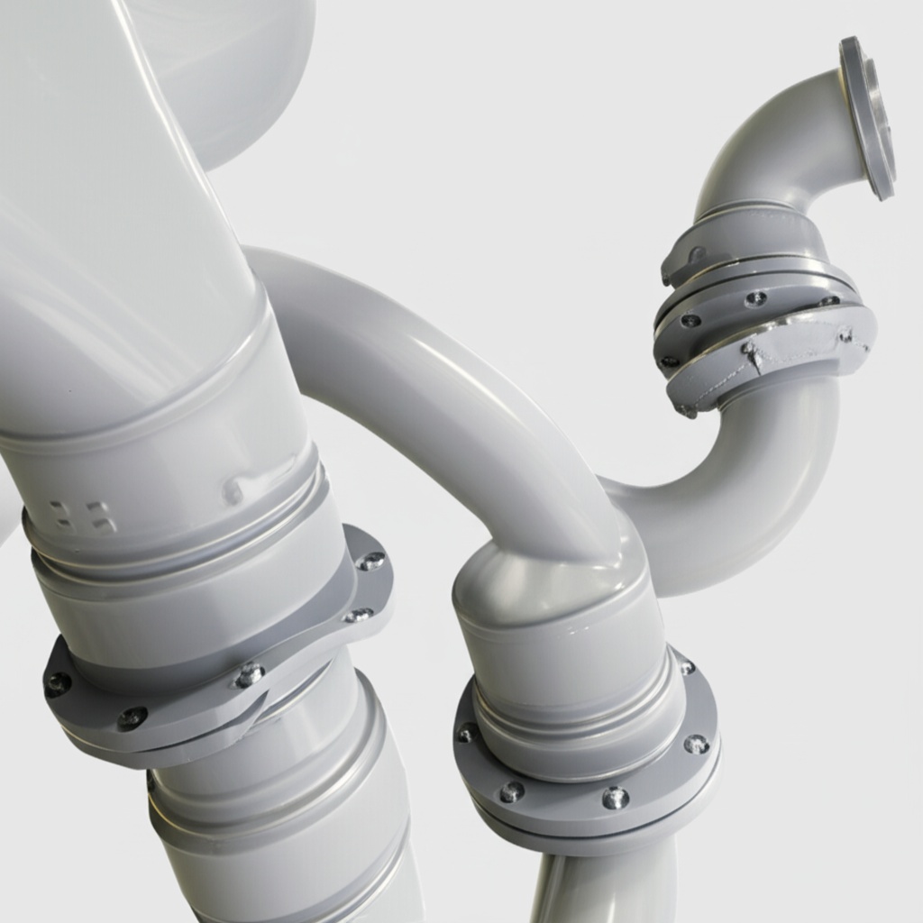
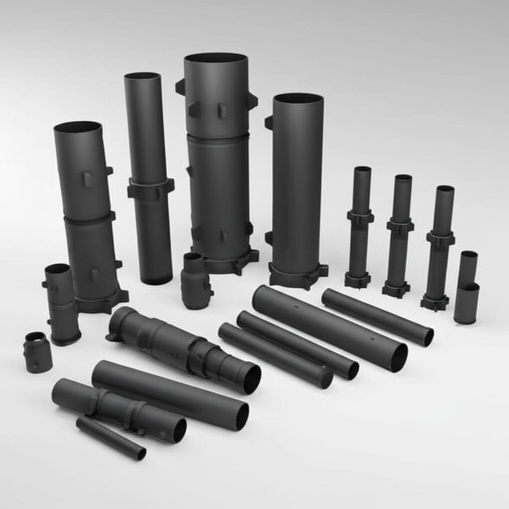
While standard, off-the-shelf Silicon Carbide components meet many needs in the semiconductor industry, the quest for optimized performance, unique form factors, and application-specific characteristics often necessitates custom SiC solutions. Customization allows engineers and designers to tailor SiC properties and geometries to their precise requirements, unlocking further efficiencies and competitive advantages. This is particularly true for specialized semiconductor manufacturing equipment parts (chucks, rings, susceptors) and advanced device substrates or epitaxial layers.
Benefits of custom SiC solutions in the semiconductor sphere include:
- Optimized Performance: Custom doping profiles, specific crystal orientations, or unique epitaxial layer structures can be designed to enhance device characteristics like breakdown voltage, on-resistance, or switching speed for a particular application.
- Specific Geometries and Form Factors: Semiconductor manufacturing involves intricate equipment where components like SiC susceptors, wafer chucks, or edge rings must fit precise dimensions. Custom fabrication ensures perfect integration and optimal thermal or plasma uniformity.
- Enhanced Thermal Management: Custom SiC heat spreaders or substrates can be designed with specific thicknesses and surface finishes to maximize thermal dissipation for high-power modules.
- Integration with Other Materials: Custom SiC components can be designed for bonding or integration with other materials, facilitating complex module assemblies.
- Improved Material Purity or Specific Grades: Some cutting-edge applications might require even higher purity levels or specific SiC polytypes not commonly available as standard products. Custom production can address these niche requirements.
Recognizing the growing demand for tailored solutions, specialized providers have emerged. A significant global hub for such expertise is located in Weifang City, China, which is home to over 40 silicon carbide production enterprises of various sizes. These enterprises collectively account for more than 80% of China’s total silicon carbide output. Within this dynamic ecosystem, Sicarb Tech stands out. Since 2015, we have been instrumental in introducing and implementing advanced silicon carbide production technology, significantly assisting local enterprises in achieving large-scale production and technological advancements. Our deep involvement has allowed us to witness and contribute to the emergence and ongoing development of this vital SiC industry hub.
Sicarb Tech, operating under the umbrella of the Chinese Academy of Sciences (Weifang) Innovation Park and in close collaboration with the National Technology Transfer Center of the Chinese Academy of Sciences , leverages the formidable scientific and technological capabilities of Chinese Academy of Sciences. We offer a robust platform for customizing SiC products, backed by a top-tier professional team specializing in the custom production of a wide array of SiC components. Our expertise spans material science, process engineering, design optimization, and meticulous measurement and evaluation technologies. This integrated approach, from raw materials to finished products, enables us to meet diverse and complex customization needs for the semiconductor industry and beyond, ensuring higher-quality and cost-competitive solutions.
Quality Assurance and Testing in SiC Components
The exceptional performance characteristics of Silicon Carbide devices can only be realized if the underlying materials and components meet stringent quality standards. For semiconductor applications, where even minute imperfections can lead to device failure or degraded performance, robust quality assurance (QA) and comprehensive testing protocols are non-negotiable. Procurement managers and engineers must prioritize suppliers who demonstrate an unwavering commitment to quality control throughout the SiC manufacturing process.
Key aspects of QA and testing for semiconductor-grade SiC components include:
- Material Characterization:
- Polytype Verification: Techniques like Raman spectroscopy or X-ray diffraction (XRD) are used to confirm the correct SiC polytype (e.g., 4H-SiC, 6H-SiC).
- Purity Analysis: Glow Discharge Mass Spectrometry (GDMS) or Secondary Ion Mass Spectrometry (SIMS) can determine trace elemental impurities.
- Resistivity Mapping: Four-point probe measurements or eddy current methods map the resistivity distribution across wafers to ensure doping uniformity.
- Defect Metrology:
- Micropipe Density (MPD): Automated optical inspection after KOH etching or non-destructive techniques like photoluminescence (PL) mapping or X-ray topography (XRT) are used to count and map micropipes.
- Dislocation Density: Similar techniques (etching, PL, XRT) are employed to quantify other dislocations like Basal Plane Dislocations (BPDs) and Threading Screw Dislocations (TSDs).
- Stacking Faults: PL imaging is particularly effective for identifying stacking faults in epilayers.
- Surface and Subsurface Quality Assessment:
- Surface Roughness: Atomic Force Microscopy (AFM) measures surface roughness at the angstrom or nanometer scale.
- Surface Contamination: Total Reflection X-ray Fluorescence (TXRF) or Vapor Phase Decomposition (VPD) followed by ICP-MS can detect surface metallic contaminants.
- Subsurface Damage: Techniques like cross-sectional Transmission Electron Microscopy (TEM) or specialized etching can reveal damage layers from grinding or polishing.
- Dimensional Metrology:
- Precise measurement of wafer diameter, thickness, bow, warp, and site flatness using automated metrology tools.
- For custom components, CMM (Coordinate Measuring Machines) or optical profilometry verify critical dimensions and tolerances.
- Epitaxial Layer Characterization:
- Thickness Uniformity: Fourier Transform Infrared Spectroscopy (FTIR) or spectroscopic ellipsometry.
- Doping Concentration and Uniformity: Capacitance-Voltage (CV) measurements, SIMS.
- Surface Morphology: Nomarski microscopy, AFM.
- Electrical Testing (for finished devices or test structures):
- On-wafer probing of parameters like breakdown voltage, on-state resistance, leakage current, and threshold voltage.
- Dynamic testing to evaluate switching characteristics.
- Process Control and Traceability:
- Statistical Process Control (SPC) throughout manufacturing.
- Lot traceability from raw material to finished product.
- Compliance with industry standards (e.g., SEMI standards for wafers).
Reliable SiC suppliers invest heavily in advanced metrology equipment and maintain rigorous QA systems. They should be able to provide comprehensive data sheets, certificates of conformity, and detailed test reports for their products. For custom components, collaborative development of a Quality Plan, outlining critical parameters and inspection methods, is often beneficial. This ensures that the final SiC product consistently meets the high-stakes demands of semiconductor manufacturing and device performance.
Future Trends: SiC Pushing Semiconductor Boundaries
The impact of Silicon Carbide on the semiconductor industry is already profound, but the technology is far from static. Ongoing research and development are continuously pushing the boundaries of SiC capabilities, promising even more exciting advancements in the years to come. For businesses in the semiconductor, automotive, aerospace, and energy sectors, staying abreast of these trends is crucial for future-proofing designs and maintaining a competitive edge.
Key future trends in SiC technology include:
- Larger Wafer Diameters: The transition from 150mm (6-inch) to 200mm (8-inch) SiC wafers is well underway. Larger wafers significantly reduce the per-die cost, making SiC devices more economically competitive with silicon. Research is also exploring the feasibility of 300mm (12-inch) SiC wafers, though this presents substantial technical challenges.
- Improved Crystal Quality and Defect Reduction: A primary focus remains on reducing defect densities (micropipes, BPDs, TSDs) in SiC substrates and epilayers. Lower defect densities lead to higher device yields, improved reliability, and the ability to manufacture larger, more powerful SiC chips.
- Advanced Epitaxy Techniques: Innovations in CVD processes, including new precursors and reactor designs, aim for faster growth rates, better uniformity over large wafers, and more precise control over doping profiles and layer thicknesses. This includes the development of thicker drift layers for ultra-high voltage devices (>10 kV).
- Novel Device Structures:
- SiC Trench MOSFETs: While planar SiC MOSFETs are common, trench gate structures offer

About the Author: Sicarb Tech
We provide clear and reliable insights into silicon carbide materials, component manufacturing, application technologies, and global market trends. Our content reflects industry expertise, practical experience, and a commitment to helping readers understand the evolving SiC landscape.

Customizable SiC
You May Also Interest
-
![]()
Precision SiC Rings for Reliable Mechanical Seals
Precision SiC Rings for Reliable Mechanical Seals In the demanding world of industrial applications, the reliability of every component is paramount. Mechanical seals play a critical role in preventing leakage, containing pressure, and excluding contaminants in rotating equipment. At the heart of these seals, the choice of material for seal faces is crucial for performance…
-
Key SiC Exporters in Asia for International Trade
Key SiC Exporters in Asia for International Trade In the rapidly evolving landscape of advanced materials, silicon carbide (SiC) stands out as a material of unparalleled performance. Its exceptional properties make it indispensable across a spectrum of demanding industrial applications. For businesses seeking reliable and high-quality silicon carbide products, understanding the key players and regions…
-
![]()
SiC Substrates: Key to Electronic Device Advances
SiC Substrates: Key to Electronic Device Advances Introduction: The Pivotal Role of SiC Substrates In the rapidly evolving landscape of high-performance industrial applications, materials science plays a crucial role. Among advanced materials, silicon carbide (SiC) stands out, particularly in the form of SiC substrates. These substrates are not merely foundational layers; they are critical enablers…