Accurate SiC Measurement Tools for Precise Results

Share
Accurate SiC Measurement Tools for Precise Results
Introduction: The Critical Role of SiC Measurement Tools
Silicon Carbide (SiC) has emerged as a cornerstone material in high-performance industrial applications, revolutionizing sectors from semiconductors and automotive to aerospace and renewable energy. Its exceptional properties, including high thermal conductivity, wide bandgap, superior hardness, and chemical inertness, make it indispensable for devices operating under extreme conditions. However, harnessing the full potential of SiC relies heavily on the ability to accurately measure and characterize its properties and the performance of SiC components. This is where silicon carbide measurement tools play a pivotal role. These specialized instruments are essential for quality control, process optimization, research and development, and ensuring the reliability and efficiency of SiC-based technologies. Without precise metrology, manufacturers risk producing substandard components, leading to device failure, increased costs, and slowed innovation. This post will delve into the world of SiC measurement tools, exploring their types, applications, and the critical importance of accuracy in today’s demanding industrial landscape.
Key SiC Properties Requiring Accurate Measurement
The performance of silicon carbide components is directly tied to a range of physical, electrical, and thermal properties. Accurate measurement of these parameters is crucial throughout the SiC lifecycle, from raw material inspection to final device testing. Key properties include:
- Electrical Properties:
- Resistivity: Critical for power electronics and semiconductor applications.
- Carrier Concentration & Mobility: Determines device speed and efficiency.
- Breakdown Voltage: Essential for high-power SiC devices.
- Interface Trap Density: Impacts MOSFET performance and reliability.
- Thermal Properties:
- Thermal Conductivity: Vital for heat dissipation in power devices and high-temperature applications.
- Thermal Expansion Coefficient: Important for material compatibility and stress management.
- Mechanical Properties:
- Hardness & Toughness: Relevant for wear-resistant components and structural ceramics.
- Elastic Modulus & Flexural Strength: Key for structural integrity.
- Surface Roughness & Flatness: Critical for wafer processing and optical applications.
- Optical Properties:
- Refractive Index & Absorption Coefficient: Important for SiC optics and sensors.
- Material Purity & Defects:
- Impurity Concentrations: Can significantly affect electrical and optical properties.
- Crystal Defects (e.g., micropipes, stacking faults): Impact device yield and long-term reliability.
- Grain Size & Distribution: Influences mechanical and thermal properties in polycrystalline SiC.
- Dimensional Metrology:
- Layer Thickness (e.g., epitaxial layers, gate oxides).
- Critical Dimensions (CD) of device features.
- Warpage and bow of SiC wafers.
Understanding and controlling these properties through precise measurement enables manufacturers to optimize their processes, improve product quality, and accelerate the development of next-generation SiC technologies.
Types of Silicon Carbide Measurement Tools and Technologies
A diverse array of measurement tools and techniques are employed to characterize silicon carbide. The choice of tool depends on the specific property being measured, the form of the SiC material (bulk, wafer, thin film, powder), and the required precision. Some common categories include:
Electrical Characterization Tools:
- Four-Point Probes & Hall Effect Systems: For measuring resistivity, carrier concentration, and mobility. These are fundamental for SiC semiconductor development.
- Capacitance-Voltage (C-V) Profilers: Used to determine doping profiles, interface states, and oxide charges in SiC MOS structures.
- Current-Voltage (I-V) Testers: Essential for characterizing diode and transistor performance, including breakdown voltage and leakage currents.
- Deep Level Transient Spectroscopy (DLTS): Identifies and characterizes electrically active defects within the SiC bandgap.
- Non-Contact Sheet Resistance Measurement Tools: Offer fast, contamination-free mapping of wafer resistivity.
Optical & Spectroscopic Tools:
- Ellipsometers: Measure thickness and optical constants of thin SiC films and dielectric layers.
- Photoluminescence (PL) & Raman Spectroscopy: Provide insights into crystal quality, defects, stress, and polytype identification.
- Fourier Transform Infrared Spectroscopy (FTIR): Used to analyze chemical bonding, impurities, and epitaxial layer thickness.
- UV-Vis-NIR Spectrophotometers: Characterize optical transmission and absorption properties.
Microscopy & Surface Analysis Tools:
- Atomic Force Microscopy (AFM): For high-resolution surface topography, roughness measurement, and mapping of electrical/mechanical properties at the nanoscale.
- Scanning Electron Microscopy (SEM) & Transmission Electron Microscopy (TEM): Visualize microstructure, defects, and perform elemental analysis (often coupled with EDX/EBSD).
- X-ray Diffraction (XRD) & X-ray Topography (XRT): Analyze crystal structure, orientation, strain, and visualize extended defects like dislocations and micropipes.
- White Light Interferometry: Provides rapid, non-contact 3D surface profiling and roughness measurements.
Thermal Analysis Tools:
- Laser Flash Analyzers (LFA): Measure thermal diffusivity and conductivity.
- Differential Scanning Calorimetry (DSC) & Thermogravimetric Analysis (TGA): Study thermal stability, phase transitions, and material composition.
Mechanical Testing Equipment:
- Indentation Testers (Nano & Micro): Determine hardness and elastic modulus.
- Flexural Strength Testers: Measure the material’s ability to resist bending forces.
Many of these tools are adapted or specifically designed to handle the unique challenges posed by SiC, such as its hardness, chemical inertness, and in some cases, the need for high-temperature measurements.
Applications: Precision SiC Measurement Across Industries
The demand for accurate SiC measurement spans numerous high-tech industries, each with specific needs and challenges.
| Industry | Key SiC Applications | Critical Measurement Needs |
|---|---|---|
| Semiconductors & Power Electronics | MOSFETs, SBDs, power modules, ICs | Epitaxial layer thickness, doping uniformity, defect density (micropipes, stacking faults), gate oxide integrity, resistivity, thermal impedance. |
| Automotive | EV inverters, on-board chargers, DC-DC converters | High-temperature electrical performance, reliability under thermal cycling, breakdown voltage, mechanical strength of packaging. |
| Aerospace & Defense | High-temperature sensors, rad-hard electronics, thruster components, mirrors | Thermal stability, radiation hardness, dimensional accuracy, surface finish, material purity. |
| Renewable Energy | Solar inverters, wind turbine converters | Efficiency, reliability, thermal management, lifetime prediction based on defect analysis. |
| LED Manufacturing | SiC substrates for GaN epitaxy | Wafer surface quality (roughness, TTV, bow/warp), crystal orientation, defect mapping. |
| Metallurgy & High-Temperature Processing | Kiln furniture, crucibles, heating elements, thermocouple protection tubes | Thermal shock resistance, chemical inertness at high temperatures, mechanical strength, creep resistance. Custom SiC components are vital here. |
| Chemical Processing | Seals, bearings, nozzles, heat exchangers | Corrosion resistance, wear resistance, dimensional stability. |
| Industrial Machinery | Wear parts, precision mechanical components | Hardness, abrasion resistance, dimensional tolerances. |
In each of these sectors, precision SiC measurement is not just a quality check but an integral part of process control, material development, and ensuring the final product meets stringent performance and reliability standards. For instance, in semiconductor manufacturing, mapping defect distributions on a SiC wafer allows for yield prediction and process adjustments, directly impacting profitability.
Why Precision Matters: Benefits of Accurate SiC Measurement
The emphasis on “precision” and “accuracy” in SiC measurement is not arbitrary. It underpins several critical benefits for manufacturers and end-users:
- Enhanced Product Quality & Reliability: Accurate measurements ensure that SiC components meet design specifications, leading to more reliable and longer-lasting end products. This is particularly crucial in safety-critical applications like automotive and aerospace.
- Improved Manufacturing Yield: By identifying material defects or process deviations early through precise metrology, manufacturers can reduce scrap rates and improve overall yield. For example, SiC wafer inspection tools can flag defective wafers before costly processing steps.
- Accelerated Research & Development: Researchers rely on accurate data to understand material behavior, develop new SiC formulations, and optimize device designs. Precision measurement tools enable faster innovation cycles.
- Optimized Process Control: Real-time or frequent measurements allow for tighter control over manufacturing processes, leading to more consistent product quality and reduced variability.
- Cost Reduction: While advanced measurement tools represent an investment, they contribute to overall cost reduction by minimizing failures, improving efficiency, and reducing material waste.
- Compliance with Standards: Many industries have stringent quality standards. Accurate measurement systems provide the data needed to demonstrate compliance and ensure interoperability.
- Supplier-Customer Trust: Clear, verifiable measurement data builds trust between SiC material/component suppliers and their customers, ensuring that specifications are met.
Ultimately, the drive for smaller, faster, and more efficient devices, especially in power electronics and high-frequency applications, pushes the limits of SiC technology. Precision measurement is the enabler that allows engineers to confidently operate at these frontiers.
Innovations in Custom SiC Measurement Solutions
As SiC applications become more complex and demanding, standard off-the-shelf measurement tools may not always suffice. This has led to a growing need for custom SiC measurement solutions and innovations in metrology techniques. Key areas of development include:
- In-situ and In-line Metrology: Developing tools that can measure SiC properties during manufacturing processes (e.g., during crystal growth or epitaxy) rather than post-process. This allows for real-time feedback and control.
- High-Throughput Wafer Mapping: Tools capable of rapidly mapping entire SiC wafers for multiple parameters (e.g., defects, resistivity, thickness uniformity) to cope with increasing production volumes.
- Non-Destructive Testing (NDT) Advances: Enhancing NDT techniques like X-ray topography, acoustic microscopy, and terahertz imaging to detect subsurface defects and internal stresses without damaging the SiC component.
- AI and Machine Learning Integration: Using AI algorithms to analyze complex measurement data, identify subtle defect patterns, predict component lifetime, and optimize measurement strategies.
- Measurement at Extreme Conditions: Developing tools and sensors capable of accurately characterizing SiC properties at very high temperatures, high voltages, or in harsh chemical environments, mimicking real-world operating conditions.
- Multi-modal Metrology: Combining multiple measurement techniques into a single platform to provide a more comprehensive understanding of the SiC material or device. For example, correlating optical defect maps with electrical test results.
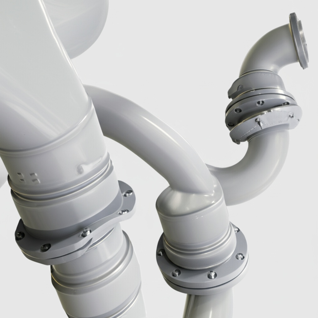
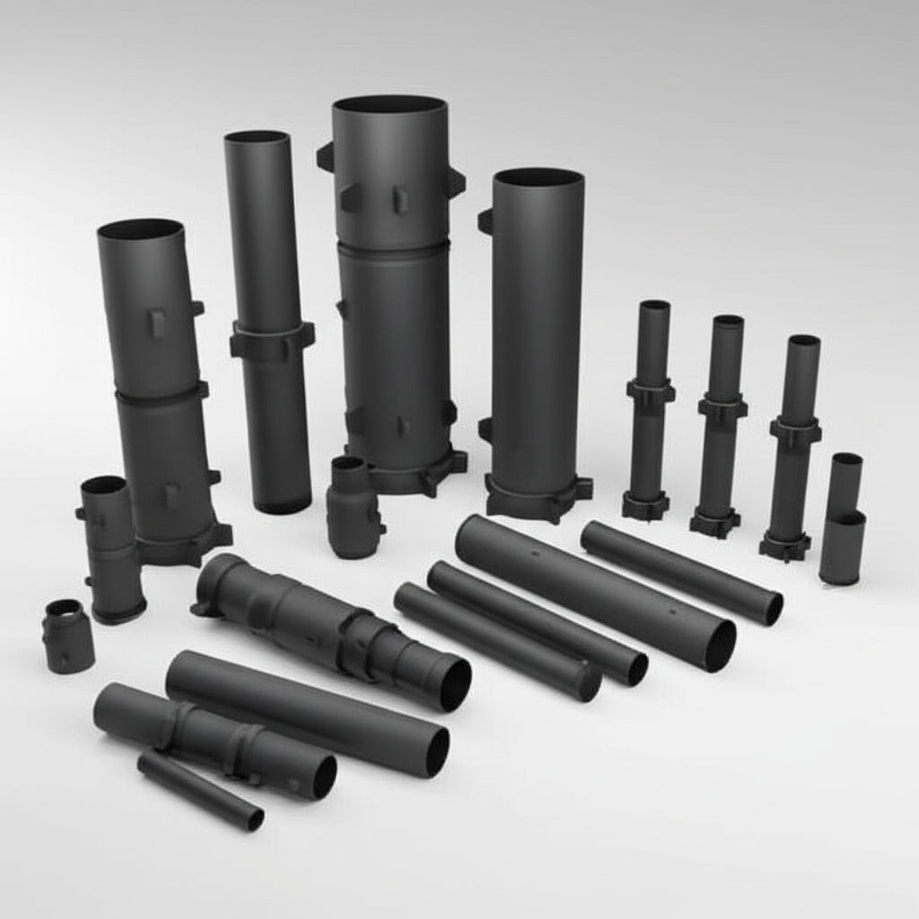
- Customized Probes and Fixtures: For unique component geometries or specific testing requirements, customized SiC measurement probes and fixtures are often necessary. These might involve SiC components themselves due to their durability and stability.
Companies specializing in advanced materials often drive these innovations. For instance, developing specific SiC probes for high-temperature applications or unique optical setups for characterizing novel SiC polytypes requires deep material science expertise alongside metrology know-how.
Design Considerations for SiC-Based Measurement Components
While this article primarily focuses on tools *for measuring* SiC, it’s also important to note that silicon carbide itself is often used to create components *within* measurement systems, especially for harsh environments or when extreme precision and stability are required. When designing such custom silicon carbide components for metrology applications, several factors are key:
- Material Grade Selection: The choice of SiC grade (e.g., sintered, reaction-bonded, CVD SiC) will depend on the required thermal stability, electrical conductivity (or insulation), wear resistance, and machinability. For instance, a probe designed for high-temperature electrical measurements might require a specific grade with stable electrical properties and minimal thermal expansion.
- Thermal Management: If the SiC component is part of a heated stage or a high-temperature probe, its thermal conductivity and emissivity must be considered in the design.
- Dimensional Stability & Tolerances: For precision positioning or optical applications, the SiC component must maintain its shape and dimensions over a range of temperatures and conditions. Tight dimensional tolerances are often required.
- Surface Finish: A smooth, well-defined surface might be necessary for optical interfaces or to ensure good contact in electrical measurements. Lapping and polishing may be required.
- Chemical Inertness: If the component will be exposed to corrosive gases or liquids during measurement, the chemical inertness of the SiC grade is paramount.
- Electrical Properties: Depending on the application, the SiC component might need to be highly insulating, semi-conducting, or conductive. Doping levels and purity will be critical.
- Manufacturability: Complex geometries can be challenging and costly to produce in SiC due to its hardness. Design for manufacturability (DFM) principles should be applied early in the design process.
Expertise in SiC material science and fabrication is crucial when designing such specialized components. This is where institutions with a strong background in material innovation and production, like those found in leading SiC manufacturing hubs, can provide significant value. Speaking of such hubs, the heart of China’s silicon carbide customizable parts manufacturing is Weifang City. This region hosts over 40 SiC production enterprises, accounting for more than 80% of China’s total SiC output.
Calibration, Standards, and Ensuring SiC Measurement Accuracy
The reliability of any measurement tool hinges on proper calibration against recognized standards. For silicon carbide metrology, ensuring accuracy involves several key aspects:
- Traceable Standards: Calibration should be performed using reference materials and standards that are traceable to national or international metrology institutes (e.g., NIST, PTB). For SiC, this can include certified reference materials for resistivity, thickness, or defect density.
- Regular Calibration Schedules: Measurement instruments drift over time due to wear, environmental changes, or electronic component aging. Regular calibration intervals, as recommended by the manufacturer or determined by internal quality procedures, are essential.
- Calibration Procedures: Following standardized calibration procedures is crucial. This may involve using specific artifacts, environmental controls, and statistical analysis of calibration data.
- Inter-laboratory Comparisons: Participating in round-robin tests or inter-laboratory comparisons can help validate a lab’s measurement capabilities and identify potential biases.
- Understanding Measurement Uncertainty: Every measurement has an associated uncertainty. It’s important to quantify this uncertainty and factor it into data interpretation and decision-making. Factors contributing to uncertainty include instrument limitations, environmental influences, operator variability, and the calibration process itself.
- Operator Training: Properly trained operators are key to minimizing errors and ensuring consistent, accurate measurements. Training should cover instrument operation, calibration, sample preparation, and data interpretation.
- Environmental Controls: Many SiC measurements are sensitive to temperature, humidity, vibration, and electromagnetic interference. Maintaining a controlled laboratory environment is often necessary.
The development of SiC-specific reference materials and standardized measurement protocols is an ongoing effort within the industry, driven by organizations like SEMI and ASTM, to further improve measurement consistency and comparability across different laboratories and manufacturers. The complexity of SiC and its various polytypes sometimes makes standardization more challenging than for traditional silicon.
Overcoming Challenges in Silicon Carbide Metrology
Measuring silicon carbide presents unique challenges due to its inherent material properties and the demanding applications it serves:
- Material Hardness & Brittleness: SiC’s extreme hardness makes it difficult to prepare samples for certain types of analysis (e.g., cross-sectioning for microscopy) and can cause wear on contact probes. Its brittleness requires careful handling.
- High-Temperature Measurements: Many SiC devices operate at elevated temperatures. Characterizing SiC properties under these conditions requires specialized equipment that can withstand high temperatures and provide accurate readings.
- Wide Bandgap Effects: The wide bandgap of SiC (e.g., ~3.2 eV for 4H-SiC) influences its electrical behavior and can make some standard semiconductor characterization techniques (developed for silicon) less effective or require modification. For example, achieving good ohmic contacts for electrical measurements can be more challenging.
- Defect Characterization: Identifying and quantifying critical defects like micropipes, basal plane dislocations, and stacking faults in SiC wafers and epilayers is crucial but can be complex. Different techniques may be needed to detect different types of defects, and correlating them with device performance is an ongoing area of research.
- Polytype Identification: SiC can exist in many different crystal structures (polytypes), each with slightly different properties. Distinguishing between polytypes, especially in mixed-polytype samples, requires techniques like Raman spectroscopy or XRD.
- Wafer Bow and Warp: SiC wafers, especially larger diameter ones, can exhibit significant bow and warp, which can complicate automated handling and some optical measurement techniques.
- Surface Contamination and Passivation: The SiC surface can be sensitive to contamination and requires careful cleaning and passivation for accurate surface-sensitive measurements.
Overcoming these challenges often involves a combination of advanced instrumentation, sophisticated analysis techniques, and deep material science expertise. Collaboration between tool vendors, SiC manufacturers, and research institutions is vital for developing new and improved metrology solutions. Sharing best practices and learning from successful case studies in SiC characterization can also help the industry advance.
Choosing Your Partner for SiC Measurement Tools & Custom Solutions
Selecting the right partner for silicon carbide measurement tools or for the development of custom SiC components for your metrology needs is a critical decision. Consider the following factors:
- Technical Expertise & Experience: Look for suppliers with proven expertise in SiC materials science, device physics, and metrology. Their team should understand the nuances of SiC characterization and the specific challenges of your application.
- Range of Solutions: Can the supplier offer a comprehensive suite of measurement tools or services relevant to your needs? For custom components, do they have diverse fabrication capabilities?
- Customization Capabilities: If you require specialized measurement setups or custom SiC components (e.g., probes, fixtures, windows), ensure the supplier has strong design and manufacturing capabilities for tailoring solutions.
- Quality and Reliability: Assess the supplier’s quality control processes, certifications, and the reputation of their instruments or components for accuracy, repeatability, and durability.
- Support and Service: Consider the level of technical support, training, calibration services, and maintenance offered. Prompt and knowledgeable support is crucial for minimizing downtime.
- Innovation and R&D Focus: A partner committed to ongoing research and development is more likely to offer cutting-edge solutions and stay ahead of evolving SiC technology requirements.
- Industry Reputation and References: Seek feedback from other customers and look for a proven track record in your industry or a related field.
Sicarb Tech offers more than just off-the-shelf products. They possess a top-tier professional team specializing in the customized production of silicon carbide products and boast a wide array of technologies spanning material science, process engineering, design, and measurement & evaluation. This integrated approach, from materials to final products, enables them to meet diverse customization needs, potentially offering higher-quality, cost-competitive custom SiC components and measurement solutions. For businesses seeking to understand these advanced capabilities, exploring options for customizing support is a valuable step.
Cost Factors and ROI in Advanced SiC Measurement
Investing in advanced silicon carbide measurement tools and solutions involves upfront costs, but it’s essential to consider the long-term return on investment (ROI). Key cost drivers include:
- Instrument Complexity and Capability: More sophisticated tools with higher precision, automation, or multi-functional capabilities will generally have a higher purchase price.
- Software and Analytical Features: Advanced data analysis software, AI-driven interpretation, and comprehensive reporting features can add to the cost.
- Customization: Custom-designed tools or components will typically be more expensive than standard off-the-shelf products.
- Calibration and Maintenance: Ongoing costs for regular calibration, preventive maintenance, and potential repairs should be factored in.
- Training: Costs associated with training personnel to operate and maintain the equipment.
- Throughput and Automation Level: Highly automated, high-throughput systems may have a higher initial cost but can lead to lower per-sample measurement costs in high-volume manufacturing.
The ROI from investing in accurate SiC measurement comes from several areas:
- Reduced Scrap & Rework: Early detection of defects and process deviations minimizes waste.
- Improved Yield: Better process control based on accurate data leads to higher yields of good devices.
- Enhanced Product Performance & Reliability: Leads to greater customer satisfaction and reduced warranty claims.
- Faster Time-to-Market: Efficient R&D and process qualification accelerate product development cycles.
- Process Optimization: Data-driven insights allow for fine-tuning manufacturing processes for optimal efficiency and quality.
- Competitive Advantage: Superior quality and reliability enabled by precision measurement can be a significant market differentiator.
When evaluating the cost, procurement managers and technical buyers should look beyond the initial purchase price and consider the total cost of ownership and the tangible benefits that improved measurement capabilities will bring to their operations and product quality. For companies considering establishing their own SiC production, the initial investment in comprehensive metrology is a critical component of ensuring success. In such cases, exploring technology transfer for professional silicon carbide production, which includes guidance on necessary measurement infrastructure, can be highly beneficial.
Frequently Asked Questions (FAQ)
- 1. What are the most critical parameters to measure for SiC power devices?
- For SiC power devices, critical parameters include epitaxial layer thickness and doping uniformity, breakdown voltage, on-state resistance (RDS(on)), leakage currents, gate oxide integrity, and the density of crystal defects such as micropipes and basal plane dislocations. Thermal resistance or impedance is also vital for ensuring effective heat dissipation.
- 2. How does the measurement of SiC wafers differ from standard silicon wafers?
- While some principles overlap, SiC wafer measurement presents unique challenges. SiC’s transparency to certain wavelengths of light requires different optical techniques. Its hardness can wear out contact probes faster. The presence of unique defects like micropipes requires specialized detection methods (e.g., X-ray topography, laser scattering). Also, the wider bandgap means electrical characterization techniques may need higher voltages or temperatures, and contact formation can be more difficult.
- 3. Can standard semiconductor metrology tools be used for SiC?
- Some standard semiconductor metrology tools can be adapted or used for certain SiC measurements, particularly for dimensional and some optical characterizations. However, for many critical SiC-specific parameters (e.g., deep-level defects, high-temperature electrical properties, certain crystal defect imaging), specialized or modified tools are often necessary to achieve accurate and reliable results. The unique properties of SiC often push standard tools beyond their intended operating ranges or capabilities.
- 4. What role does Sicarb Tech play in SiC measurement and customization?
- Sicarb Tech, leveraging its connection with the Chinese Academy of Sciences and its base in Weifang, China’s SiC manufacturing hub, offers significant expertise in silicon carbide. They provide customized SiC components and possess a range of technologies, including measurement and evaluation technologies. This allows them to support diverse customization needs for SiC products, potentially including specialized components for measurement systems or int

About the Author: Sicarb Tech
We provide clear and reliable insights into silicon carbide materials, component manufacturing, application technologies, and global market trends. Our content reflects industry expertise, practical experience, and a commitment to helping readers understand the evolving SiC landscape.

Customizable SiC
You May Also Interest
-
![]()
Precision SiC Rings for Reliable Mechanical Seals
Precision SiC Rings for Reliable Mechanical Seals In the demanding world of industrial applications, the reliability of every component is paramount. Mechanical seals play a critical role in preventing leakage, containing pressure, and excluding contaminants in rotating equipment. At the heart of these seals, the choice of material for seal faces is crucial for performance…
-
![]()
Key SiC Exporters in Asia for International Trade
Key SiC Exporters in Asia for International Trade In the rapidly evolving landscape of advanced materials, silicon carbide (SiC) stands out as a material of unparalleled performance. Its exceptional properties make it indispensable across a spectrum of demanding industrial applications. For businesses seeking reliable and high-quality silicon carbide products, understanding the key players and regions…
-
![]()
SiC Substrates: Key to Electronic Device Advances
SiC Substrates: Key to Electronic Device Advances Introduction: The Pivotal Role of SiC Substrates In the rapidly evolving landscape of high-performance industrial applications, materials science plays a crucial role. Among advanced materials, silicon carbide (SiC) stands out, particularly in the form of SiC substrates. These substrates are not merely foundational layers; they are critical enablers…