SiC in Semiconductors: A Clear Power Advantage
Share
SiC in Semiconductors: A Clear Power Advantage
1. Introduction: The Unseen Hero – Silicon Carbide in Modern Semiconductors
In the relentless pursuit of more powerful, efficient, and compact electronic devices, the semiconductor industry is undergoing a significant material evolution. While traditional silicon (Si) has been the bedrock of electronics for decades, its physical limitations are becoming increasingly apparent, especially in high-power, high-frequency, and high-temperature applications. Enter Silicon Carbide (SiC), a compound semiconductor material emerging as an unseen hero, driving the next wave of innovation. Custom silicon carbide products are rapidly becoming essential in high-performance industrial applications, particularly within the demanding realm of semiconductor manufacturing and device fabrication. This wide-bandgap semiconductor offers a unique combination of properties—superior thermal conductivity, higher breakdown electric field strength, and greater electron saturation velocity—that translates into tangible benefits for power electronics, electric vehicles, renewable energy systems, and advanced communication technologies. As we delve deeper, we will explore why SiC is not just an alternative, but a fundamental enabler for the future of the semiconductor world, offering a clear power advantage that is reshaping industries. For cutting-edge solutions, exploring a premier silicon carbide manufacturing hub can be a game-changer.
2. Powering Progress: Why SiC is Revolutionizing Semiconductor Devices
Silicon Carbide’s ascent in the semiconductor landscape is not merely an incremental improvement; it’s a revolutionary leap. Its intrinsic material properties allow for the creation of semiconductor devices that operate at significantly higher voltages, temperatures, and frequencies than their silicon-based counterparts. This translates directly into enhanced performance and efficiency in a multitude of applications.
Key Advantages Driving the SiC Revolution:
- Higher Voltage Operation: SiC possesses a breakdown electric field strength approximately ten times greater than silicon. This allows SiC devices to block much higher voltages in a smaller chip area, leading to more compact and efficient high-voltage power converters and inverters. This is critical for applications like electric vehicle (EV) drivetrains, industrial motor drives, and grid-scale power systems.
- Superior Thermal Management: With a thermal conductivity about three times higher than silicon, SiC devices can dissipate heat more effectively. This means they can operate at higher temperatures without degradation, reducing the need for bulky and expensive cooling systems. The implications for power density and system reliability are profound.
- Increased Switching Frequencies: SiC devices can switch on and off much faster than silicon devices with lower energy losses. Higher switching frequencies enable the use of smaller passive components (inductors and capacitors) in power conversion circuits, leading to a reduction in the overall size, weight, and cost of the system. This is particularly beneficial in switched-mode power supplies (SMPS) and EV fast chargers.
- Lower Energy Losses: The combination of lower on-resistance and reduced switching losses in SiC MOSFETs and Schottky diodes results in significantly higher energy efficiency. For example, in EV inverters, this can translate to increased driving range. In data centers, it means lower electricity consumption and reduced operational costs.
- Enhanced Durability and Reliability: SiC’s inherent robustness allows devices to withstand harsher operating conditions, including higher temperatures and radiation levels. This makes SiC an ideal candidate for demanding applications in aerospace, defense, and downhole oil and gas exploration.
The transition to SiC is enabling breakthroughs in power electronics. For instance, SiC-based inverters in solar energy systems improve conversion efficiency, maximizing energy harvest. In automotive applications, SiC is paving the way for lighter, more efficient electric vehicles with faster charging capabilities. The overall impact is a significant step towards a more energy-efficient and technologically advanced future, all underpinned by the remarkable properties of silicon carbide for semiconductors.
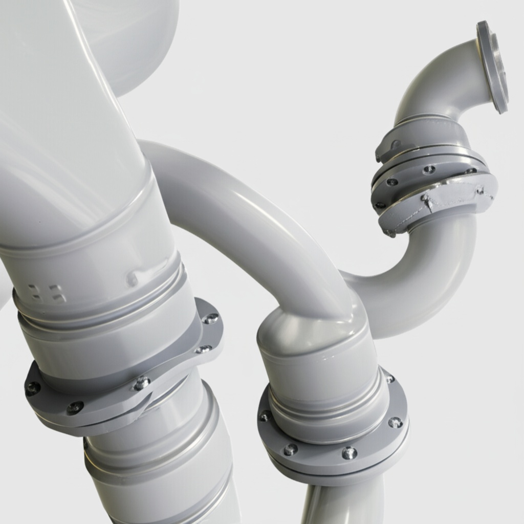
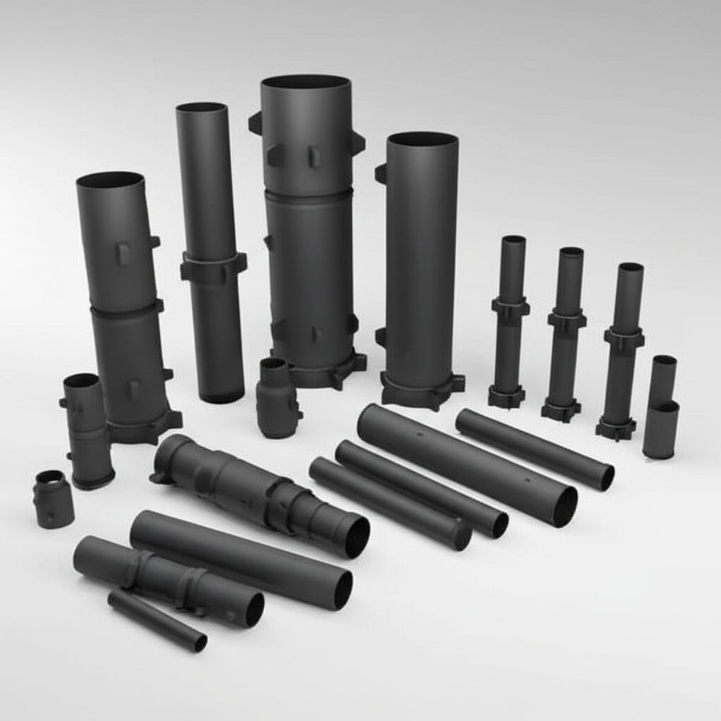
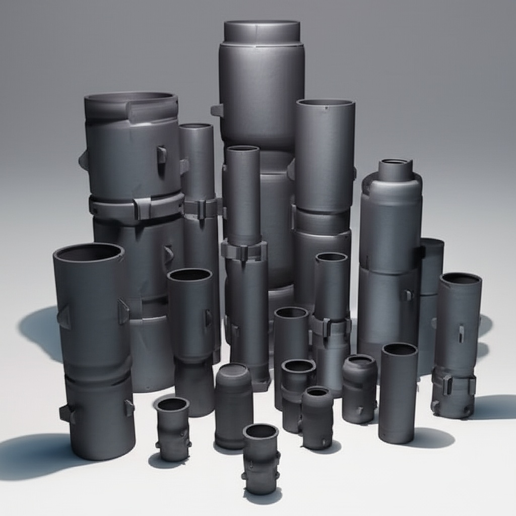
3. The Custom Advantage: Tailoring SiC for Peak Semiconductor Performance
While off-the-shelf SiC components serve many purposes, the true potential of silicon carbide in demanding semiconductor manufacturing processes is often unlocked through customization. Semiconductor fabrication involves highly precise and often aggressive environments, requiring components that meet exact specifications for geometry, purity, thermal performance, and chemical resistance. Custom SiC components are engineered to address these specific needs, delivering peak performance where standard parts might falter.
Benefits of Custom Silicon Carbide in Semiconductor Applications:
- Optimized Thermal Management: Semiconductor processes like etching, deposition, and ion implantation generate significant heat. Custom SiC components, such as wafer chucks (electrostatic or vacuum), susceptors, and heating elements, can be designed with specific thermal conductivity profiles and geometries to ensure uniform temperature distribution across the wafer, minimizing defects and improving yield.
- Enhanced Electrical Properties: For applications like electrostatic chucks (ESCs), the electrical resistivity and dielectric properties of SiC are critical. Customization allows for tuning these properties to achieve optimal wafer clamping force and prevent arcing or particle generation. High-purity SiC can also minimize metallic contamination.
- Superior Chemical Inertness and Plasma Resistance: Plasma etch and chemical vapor deposition (CVD) processes utilize highly corrosive gases and plasmas. Custom SiC components like etch rings, showerheads, and chamber liners can be fabricated from specific SiC grades (e.g., high-purity CVD SiC) that offer exceptional resistance to these harsh environments, leading to longer component lifetimes and reduced contamination.
- Precision Geometries and Complex Designs: Modern semiconductor equipment demands intricate component designs for gas flow dynamics, plasma confinement, and wafer handling. Advanced manufacturing techniques allow for the creation of custom SiC parts with complex shapes, tight tolerances, and specific surface finishes, ensuring seamless integration and optimal process performance. Explore our customizing support for your specific SiC needs.
- Improved Process Yield and Throughput: By using components tailored to the specific requirements of a process step, manufacturers can reduce downtime, minimize wafer contamination, and improve the consistency of their operations. This directly translates to higher yields and increased throughput.
- Extended Component Lifespan: Custom SiC parts, designed with the application’s specific wear mechanisms in mind (e.g., erosion, corrosion, thermal cycling), can offer significantly longer service life compared to generic alternatives, reducing the total cost of ownership.
The ability to tailor material composition, microstructure, and component design makes custom silicon carbide an indispensable asset for semiconductor manufacturers striving for higher efficiency, improved yields, and the capability to produce next-generation integrated circuits. Procurement managers and technical buyers in the semiconductor industry increasingly recognize the long-term value and competitive edge provided by investing in these specialized SiC solutions.
4. Decoding SiC Grades: Selecting the Right Material for Semiconductor Applications
Silicon Carbide is not a monolithic material; it encompasses a family of materials, each with distinct properties derived from its manufacturing process and microstructure. Selecting the appropriate SiC grade is paramount for optimizing performance and longevity in specific semiconductor applications. Understanding these distinctions is crucial for engineers and procurement professionals.
Key SiC Grades Relevant to Semiconductor Manufacturing:
- CVD-SiC (Chemical Vapor Deposition Silicon Carbide):
- Properties: Extremely high purity (often >99.9995%), theoretically dense, excellent chemical resistance (especially to etching gases like fluorine and chlorine plasmas), good thermal shock resistance, and the ability to form complex shapes via coating onto graphite or other formers. Can also be produced as thick, free-standing material.
- Semiconductor Applications: Critical plasma etch chamber components (showerheads, focus rings, liners, baffle plates), susceptors for epitaxial reactors, RTP (Rapid Thermal Processing) components, dummy wafers, and optical components. Its high purity minimizes particulate and metallic contamination.
- SSiC (Sintered Silicon Carbide):
- Direct Sintered SiC (Pressureless Sintered): Produced by sintering fine SiC powder with non-oxide sintering aids (like boron and carbon) at high temperatures (2000-2200°C).
- Properties: High density (typically >98% theoretical), excellent strength and hardness, good wear resistance, good thermal conductivity, and good chemical resistance. Purity is generally lower than CVD-SiC but can be very high depending on raw materials and processing.
- Semiconductor Applications: Wafer chucks (heaters, ESCs), structural components, wear parts, some types of susceptors, end effectors for wafer handling robots, and kiln furniture for thermal processing.
- LPSSiC (Liquid Phase Sintered SiC): Uses oxide additives that form a liquid phase during sintering, allowing for lower sintering temperatures and potentially near-net shaping.
- Properties: Can achieve high density, but properties can be influenced by the intergranular liquid phase. Often tailored for specific electrical or thermal properties.
- Semiconductor Applications: Specialized heaters, components requiring tailored electrical resistivity.
- Direct Sintered SiC (Pressureless Sintered): Produced by sintering fine SiC powder with non-oxide sintering aids (like boron and carbon) at high temperatures (2000-2200°C).
- RBSiC (Reaction-Bonded Silicon Carbide / Silicon Infiltrated Silicon Carbide – SiSiC):
- Properties: Made by infiltrating a porous SiC and carbon preform with molten silicon. Contains free silicon (typically 8-20%), which limits its maximum operating temperature (around 1350°C) and chemical resistance in certain aggressive environments (e.g., strong alkalis or hydrofluoric acid). However, it offers good thermal shock resistance, high thermal conductivity, and excellent wear resistance. Easier to produce complex shapes at lower cost than SSiC.
- Semiconductor Applications: Less common in direct plasma-facing applications due to free silicon. Used for structural components, jigs, fixtures, heat exchangers, and some kiln furniture where extreme purity or resistance to highly corrosive plasmas is not the primary concern. Can be cost-effective for larger components.
- Nitride-Bonded Silicon Carbide (NBSiC):
- Properties: SiC grains bonded by a silicon nitride (Si3N4) matrix. Good thermal shock resistance, moderate strength, and good resistance to wetting by molten metals.
- Semiconductor Applications: Primarily used in non-critical thermal processing applications, such as kiln furniture, thermocouple protection tubes, where high purity is not paramount.
Table: Comparison of Common SiC Grades for Semiconductor Use
| Property | CVD-SiC | SSiC (Direct Sintered) | RBSiC (SiSiC) |
|---|---|---|---|
| Purity | Very High (≥99.9995%) | High (≥98.5%, can be higher) | Moderate (contains free Si) |
| Density (% Theoretical) | ~100% | >98% | >99% (includes free Si) |
| Max. Use Temperature | ~1600-1800°C (inert atm.) | ~1600-1700°C (inert atm.) | ~1350°C (due to free Si) |
| Thermal Conductivity (W/mK) | 120-250 (depends on structure) | 80-150 | 100-180 |
| Plasma Erosion Resistance | Excellent | Good to Very Good | Fair to Good (Si can be selectively etched) |
| Cost | High to Very High | Moderate to High | Low to Moderate |
| Typical Semiconductor Applications | Etch chamber parts, susceptors, RTP parts, showerheads | Wafer chucks, structural parts, heating elements, end effectors | Jigs, fixtures, heat exchangers (less critical areas) |
The choice of SiC grade will depend on a careful analysis of the application’s operating conditions, performance requirements, and cost considerations. Collaborating with an experienced SiC supplier who understands these nuances is vital for success.
5. Precision by Design: Engineering Custom SiC Components for Semiconductor Tools
The intricate processes within semiconductor manufacturing tools demand components engineered with unparalleled precision. Custom Silicon Carbide parts play a pivotal role here, but their effectiveness hinges on meticulous design considerations that balance performance requirements with manufacturability. Engineers must consider the unique properties of SiC and the specific environment the component will face.
Key Design Considerations for Custom SiC Semiconductor Components:
- Material Grade Selection: As discussed previously, the choice of SiC grade (CVD, SSiC, etc.) is foundational. The design must align with the chosen grade’s capabilities and limitations in terms of purity, thermal expansion, electrical resistivity, and chemical resistance.
- Thermal Management Strategy:
- Uniformity: For components like susceptors or electrostatic chucks (ESCs) with integrated heaters, the design must ensure uniform temperature distribution across the wafer surface (e.g., ±1°C). This involves careful placement of heating elements, thermal breaks, or cooling channels if applicable.
- Thermal Expansion Mismatch: SiC has a relatively low coefficient of thermal expansion (CTE). When interfacing with other materials (metals, other ceramics), CTE mismatch must be managed to prevent stress buildup and potential failure during thermal cycling. Design features like compliant layers or specific mounting schemes may be necessary.
- Heat Dissipation: For components that generate or are exposed to high heat loads, the design should facilitate efficient heat removal to prevent overheating and maintain process stability.
- Electrical Design (for ESCs, Heaters, RF transparent parts):
- Resistivity Control: For ESCs, the SiC’s resistivity must be precisely controlled to achieve the desired clamping force (Johnson-Rahbek effect or Coulombic). Doping or specific SSiC formulations are used.
- Dielectric Strength: Components exposed to high voltages must be designed to prevent dielectric breakdown. Edge terminations, material purity, and surface finish are critical.
- RF Transparency/Coupling: For plasma processing components, the SiC material might need to be transparent to RF or microwave energy or, conversely, act as an electrode. Material choice and geometry play key roles.
- Mechanical Integrity and Manufacturability:
- Brittleness: SiC is a hard but brittle ceramic. Designs should avoid sharp internal corners, stress concentrators, and thin, unsupported sections where possible. Generous radii and chamfers are recommended. Finite Element Analysis (FEA) is often used to predict stress distributions.
- Geometric Complexity: While advanced forming techniques (e.g., slip casting, isopressing for SSiC; CVD coating for complex graphite mandrels) allow for intricate shapes, overly complex designs can significantly increase manufacturing cost and lead time. Design for Manufacturability (DfM) principles are crucial.
- Machinability: Post-sintering or post-deposition machining of SiC is challenging and expensive due to its hardness. Designs should minimize the need for extensive hard machining where feasible. Near-net-shape forming is preferred.
- Gas Flow Dynamics and Plasma Interaction:
- Showerheads: Hole pattern, size, and aspect ratio are critical for uniform gas distribution in CVD and etch processes.
- Focus Rings/Confinement Rings: Dimensions and profiles directly impact plasma density and uniformity over the wafer.
- Surface Roughness and Porosity: A smooth, non-porous surface is generally desired to minimize particle generation and ensure easy cleaning.
- Interface Compatibility and Sealing: Components often need to seal against other parts of the vacuum chamber or process tool. The design of sealing surfaces and compatibility with sealing materials (e.g., O-rings, metal seals) is important.
Engineering custom SiC components for semiconductor tools is a collaborative effort between the end-user and the SiC manufacturer. Early engagement with a knowledgeable supplier can help optimize designs for performance, reliability, and cost-effectiveness, ensuring the final product meets the stringent demands of advanced semiconductor fabrication.
6. Achieving Perfection: Tolerances, Surface Finish, and Purity in SiC for Semiconductors
In the microelectronics world, precision is not just a goal; it’s a fundamental requirement. For Silicon Carbide components used in semiconductor manufacturing, achieving stringent dimensional tolerances, exceptionally smooth surface finishes, and ultra-high purity levels is critical for process integrity, yield, and device performance. These parameters directly impact wafer quality, particulate contamination, and component longevity.
Dimensional Tolerances:
- Tight Control: Semiconductor equipment parts often require dimensional tolerances in the micron (µm) range. For example, the flatness of a wafer chuck or susceptor is critical for uniform heat transfer and consistent wafer processing. Positional accuracy of features like gas holes in a showerhead or alignment pins also demands high precision.
- Manufacturing Capabilities: Achieving such tight tolerances on hard ceramics like SiC requires advanced manufacturing processes. Green machining (before sintering) can provide initial shaping, but final precision is typically achieved through diamond grinding, lapping, and polishing of the densified SiC material.
- Metrology: Sophisticated metrology tools, including Coordinate Measuring Machines (CMMs), optical profilometers, and interferometers, are essential to verify that components meet the specified dimensional and geometric tolerances (e.g., flatness, parallelism, cylindricity).
Surface Finish (Roughness):
- Minimizing Particle Generation: A smooth surface (low Ra, Rq, Rz values) is crucial to prevent particle adhesion and subsequent shedding, which can cause killer defects on wafers. Typical requirements for critical SiC components can be Ra < 0.4 µm, and often much lower (e.g., Ra < 0.1 µm or even Angstrom-level smoothness for CMP applications).
- Process Compatibility: In plasma etch or CVD processes, a smooth surface can also improve resistance to chemical attack and make cleaning procedures more effective. For optical applications (e.g., SiC mirrors or windows), surface roughness directly impacts reflectivity and scatter.
- Achievable Finishes:
- As-fired/As-deposited: Surface finish depends on the forming process. CVD SiC typically has a smoother as-deposited surface than sintered SiC.
- Ground: Diamond grinding can achieve Ra values in the range of 0.2 to 0.8 µm.
- Lapped: Lapping with fine diamond abrasives can improve surface finish to Ra ~0.05 to 0.2 µm.
- Polished: Chemical Mechanical Polishing (CMP) or specialized diamond polishing techniques can achieve optical-grade finishes with Ra < 0.01 µm (10 nm) or even lower for super-polished surfaces.
Purity Levels:
- Contamination Control: Metallic and organic contaminants are anathema in semiconductor fabrication. Even trace impurities (ppb or ppt levels) leached from equipment components can diffuse into silicon wafers, altering their electrical properties and leading to device failure.
- High-Purity Grades: CVD-SiC is favored for its intrinsic high purity. High-purity SSiC, processed using carefully selected raw materials and cleanroom environments, is also used. The focus is on minimizing mobile ions (Na, K, Fe, Cu, etc.).
- Cleaning and Packaging: Final cleaning procedures (e.g., using ultrapure deionized water, specialized chemistries, and plasma cleaning) are critical. Components are typically packaged in cleanroom-compatible materials to prevent recontamination during shipping and handling.
- Certification: Suppliers often provide Certificates of Conformance (CoC) or Certificates of Analysis (CoA) detailing purity levels and critical dimensions.
The pursuit of perfection in these three areas—tolerances, surface finish, and purity—is a hallmark of high-quality SiC components for the semiconductor industry. Technical buyers and engineers should scrutinize a supplier’s capabilities in machining, finishing, cleaning, and metrology to ensure components will meet the exacting standards of modern fabs.
7. Beyond Fabrication: Essential Post-Processing for SiC Semiconductor Parts
The journey of a custom Silicon Carbide component for semiconductor applications doesn’t end with its initial forming or sintering. To meet the stringent performance, purity, and dimensional requirements of the industry, a series of meticulous post-processing steps are often essential. These operations transform a near-net-shape SiC blank into a high-precision, functional part ready for integration into sophisticated semiconductor manufacturing equipment.
Common Post-Processing Techniques for SiC Semiconductor Components:
- Precision Grinding:
- Purpose: To achieve tight dimensional tolerances, flatness, parallelism, and specific geometric features on densified SiC. Due to SiC’s extreme hardness (Mohs 9.0-9.5), diamond grinding wheels are exclusively used.
- Process: Involves surface grinding, cylindrical grinding (ID/OD), and profile grinding. Coolants are used to manage heat and remove debris.
- Outcome: Dimensions typically within tens of microns, with good surface finish (e.g., Ra 0.2-0.8 µm).
- Lapping:
- Purpose: To further improve surface finish and flatness beyond what grinding can typically achieve. Essential for sealing surfaces or components requiring intimate contact.
- Process: Components are moved between one or two lapping plates with a diamond slurry. The abrasive action removes minute amounts of material, creating a very flat and smooth surface.
- Outcome: Surface finishes of Ra ~0.05-0.2 µm and exceptional flatness.
- Polishing (including Chemical Mechanical Polishing – CMP):
- Purpose: To achieve ultra-smooth, mirror-like surfaces with minimal subsurface damage. Critical for optical components, some ESC surfaces, and applications demanding the lowest possible particle generation.
- Process: Mechanical polishing uses progressively finer diamond abrasives. CMP combines chemical etching with mechanical abrasion using a specialized slurry and pad.
- Outcome: Surface roughness can reach Ra < 0.01 µm (10 nm), sometimes down to Angstrom levels.
- Edge Profiling and Chamfering:
- Purpose: To remove sharp edges which can be sources of stress concentration, chipping, or particle generation. Chamfered or radiused edges improve handling safety and component durability.
- Process: Specialized diamond tooling is used to create precise edge profiles.
- Drilling and Hole Making:
- Purpose: Creating through-holes or blind holes for gas passage (e.g., showerheads), mounting, or sensor integration.
- Process: Diamond drilling, ultrasonic machining, or laser drilling can be employed, depending on hole size, aspect ratio, and tolerance requirements.
- Cleaning and Surface Treatment:
- Purpose: To remove any residues from machining, handling, organic contaminants, and particulates to meet stringent semiconductor purity standards.
- Process: Multi-stage cleaning processes involving ultrasonic baths with DI water, specialized detergents, acids, or solvents. Plasma cleaning (e.g., Ar or O2 plasma) can be used for final organic removal. Surface passivation might also be applied.
- Specialized Coatings (Optional):
- Purpose: To further enhance specific properties like erosion resistance, electrical characteristics, or to provide a functional surface.
- Examples: Thin CVD SiC coatings on SSiC parts for enhanced purity, or application of other ceramic or metallic layers for specific functionalities.
- Annealing:
- Purpose: To relieve internal stresses induced during machining or to stabilize the material’s microstructure.
- Process: Controlled heating and cooling cycles in a specific atmosphere.
- Inspection and Metrology:
- Purpose: Final quality assurance to verify all dimensional, surface, and purity specifications are met.
- Process: Utilizes CMMs, optical profilometers, SEM/EDX (for surface analysis and contamination checks), and other advanced inspection tools.
Each post-processing step adds value and cost but is indispensable for ensuring the SiC component performs reliably in its intended semiconductor application. Procurement managers and engineers should discuss these requirements in detail with their SiC supplier to ensure the final product is fit for purpose and meets all quality criteria.
8. Navigating Challenges: Optimizing SiC Integration in Semiconductor Manufacturing
While the advantages of Silicon Carbide in semiconductor manufacturing are compelling, its successful integration is not without challenges. Understanding these potential hurdles and implementing strategies to overcome them is key for OEMs, technical procurement professionals, and fab engineers aiming to leverage SiC’s full potential.
Common Challenges and Mitigation Strategies:
- Material Cost:
- Challenge: High-purity SiC, especially CVD-SiC and some grades of SSiC, can be significantly more expensive than traditional materials like alumina, quartz, or even lower-grade ceramics. This is due to complex raw material processing, energy-intensive manufacturing (high temperatures for sintering or deposition), and precision machining.
- Mitigation:
- Value Engineering: Focus on the total cost of ownership (TCO) rather than just initial price. Longer component lifetime, reduced downtime, and improved process yields from SiC can offset higher upfront costs.
- Grade Selection: Use the most cost-effective SiC grade that meets the application’s minimum requirements. Avoid over-specifying.
- Design Optimization: Simplify designs where p

About the Author: Sicarb Tech
We provide clear and reliable insights into silicon carbide materials, component manufacturing, application technologies, and global market trends. Our content reflects industry expertise, practical experience, and a commitment to helping readers understand the evolving SiC landscape.

Customizable SiC
You May Also Interest
-
![]()
Precision SiC Rings for Reliable Mechanical Seals
Precision SiC Rings for Reliable Mechanical Seals In the demanding world of industrial applications, the reliability of every component is paramount. Mechanical seals play a critical role in preventing leakage, containing pressure, and excluding contaminants in rotating equipment. At the heart of these seals, the choice of material for seal faces is crucial for performance…
-
![]()
Key SiC Exporters in Asia for International Trade
Key SiC Exporters in Asia for International Trade In the rapidly evolving landscape of advanced materials, silicon carbide (SiC) stands out as a material of unparalleled performance. Its exceptional properties make it indispensable across a spectrum of demanding industrial applications. For businesses seeking reliable and high-quality silicon carbide products, understanding the key players and regions…
-
![]()
SiC Substrates: Key to Electronic Device Advances
SiC Substrates: Key to Electronic Device Advances Introduction: The Pivotal Role of SiC Substrates In the rapidly evolving landscape of high-performance industrial applications, materials science plays a crucial role. Among advanced materials, silicon carbide (SiC) stands out, particularly in the form of SiC substrates. These substrates are not merely foundational layers; they are critical enablers…