Nano SiC: Unlocking New Material Possibilities

Share
Nano SiC: Unlocking New Material Possibilities
Introduction: The Dawn of Nano Silicon Carbide
In the relentless pursuit of materials that can push the boundaries of performance, nano silicon carbide (nano SiC) emerges as a game-changing advanced ceramic. Unlike its bulk counterpart, nano SiC, with particle sizes typically below 100 nanometers, exhibits significantly enhanced mechanical, thermal, optical, and chemical properties. This remarkable improvement stems from the quantum effects and increased surface area inherent at the nanoscale. For industries demanding exceptional durability, efficiency, and operational stability under extreme conditions, nano SiC offers unprecedented opportunities. From semiconductor manufacturing to aerospace engineering and power electronics, the integration of nano SiC is not merely an upgrade but a transformative step towards next-generation technologies. These advanced ceramic materials are pivotal for creating components that are lighter, stronger, and more resilient, making them essential for high-performance industrial applications. The unique attributes of nano SiC, such as superior wear resistance, high thermal conductivity, and excellent chemical inertness, are driving innovation across a multitude of sectors, positioning it as a cornerstone material for future technological advancements. Procurement managers and technical buyers seeking custom silicon carbide solutions will find nano SiC a compelling option for their most challenging applications.
The precision and unique characteristics of nano SiC particles allow for the development of materials with tailored functionalities. This opens doors for applications previously deemed impossible, enabling engineers to design systems that operate at higher temperatures, withstand harsher environments, and deliver superior performance. As we delve deeper into the capabilities of this nanomaterial, its role in driving industrial innovation becomes increasingly evident, making it a key focus for research and development globally. Explore the possibilities at Sicarb Tech to see how nano SiC can revolutionize your applications.
Unveiling the Potential: Key Applications of Nano SiC
The exceptional properties of nano silicon carbide translate into a wide array of applications across demanding industries. Its versatility allows for integration into various forms, including powders, coatings, composites, and sintered parts, each tailored for specific performance requirements.
- Semiconductor Manufacturing: Nano SiC is used in wafer handling components, polishing slurries for chemical mechanical planarization (CMP), and as a material for high-frequency, high-power devices due to its wide bandgap and high thermal conductivity. Precision SiC components are crucial here.
- Automotive Industry: Employed in high-performance braking systems, wear-resistant engine components, and as reinforcement in lightweight composites. For electric vehicles (EVs), nano SiC plays a role in power modules for inverters and converters, enhancing efficiency and thermal management.
- Aerospace and Defense: Utilized for manufacturing lightweight armor, components for hypersonic vehicles, mirrors for optical systems, and parts for rocket nozzles and propulsion systems that require extreme thermal shock resistance and high-temperature stability.
- Power Electronics: A key material for next-generation power devices, including MOSFETs and Schottky diodes, enabling higher switching frequencies, lower energy losses, and increased power density. SiC for power modules is a rapidly growing market.
- Renewable Energy: In solar and wind energy systems, nano SiC components improve the efficiency and durability of inverters and power converters. Its high thermal conductivity helps in managing heat in concentrated solar power systems.
- Metallurgy and High-Temperature Processing: Used in crucibles, heating elements, furnace linings, and thermocouple protection tubes due to its excellent high-temperature strength and resistance to corrosive environments.
- Chemical Processing: Components like seals, pump parts, and valve components made from or coated with nano SiC offer superior chemical inertness and wear resistance when handling aggressive chemicals.
- LED Manufacturing: Nano SiC can be used as a substrate material or as an additive in encapsulants to improve thermal management and light extraction efficiency in high-brightness LEDs.
- Industrial Machinery: For manufacturing wear-resistant nozzles, cutting tools, bearings, and mechanical seals, extending the lifespan and performance of equipment.
- Medical Devices: Biocompatible nano SiC coatings are being explored for medical implants and surgical tools due to their hardness and wear resistance.
- Oil and Gas: Used in downhole tools and components exposed to abrasive and corrosive conditions, enhancing durability and reliability.
This broad spectrum of applications underscores the importance of nano SiC as a critical enabling material for industries striving for higher performance, efficiency, and sustainability. The demand for custom nano SiC parts is growing as more engineers recognize its potential.
Why Opt for Nano Silicon Carbide? The Nanoscale Advantage
Choosing nano silicon carbide over conventional materials, or even its micro-scale SiC counterpart, offers a distinct set of advantages rooted in its nanoscale structure. These benefits are particularly crucial for applications where standard materials fall short.
Key advantages include:
- Enhanced Mechanical Properties:
- Superior Hardness and Wear Resistance: Nano SiC particles can create surfaces with extremely high hardness, leading to exceptional resistance to abrasion, erosion, and wear. This translates to longer component life and reduced maintenance in demanding applications like cutting tools and mechanical seals.
- Increased Strength and Toughness: When incorporated into composites or sintered into dense parts, nano SiC can improve the fracture toughness and flexural strength of materials, making them more resilient to mechanical stresses.
- Improved Thermal Properties:
- High Thermal Conductivity: Nano SiC often exhibits better thermal conductivity compared to bulk SiC, facilitating efficient heat dissipation. This is critical for thermal management in electronics, LEDs, and high-temperature processing equipment.
- Excellent Thermal Shock Resistance: The fine grain structure achieved with nano SiC can enhance a material’s ability to withstand rapid temperature changes without cracking or failing.
- Advanced Optical and Electrical Characteristics:
- Tunable Electrical Properties: The electrical conductivity of SiC can be controlled, and at the nanoscale, specific properties can be targeted for applications like sensors or specialized semiconductor devices.
- Unique Optical Properties: Nano SiC particles can have distinct optical absorption and emission characteristics, useful in certain optical components or as fluorescent markers.
- Superior Chemical Inertness and Stability:
- Exceptional Corrosion Resistance: Nano SiC maintains silicon carbide’s inherent resistance to a wide range of acids, alkalis, and molten salts, even at elevated temperatures. The dense structures achievable with nano SiC can further reduce permeability to corrosive agents.
- Enhanced Sintering Behavior:
- Lower Sintering Temperatures: The high surface area of nanoparticles can promote densification at lower temperatures compared to micro-sized powders, potentially reducing energy consumption and cost during manufacturing.
- Finer Microstructures: Sintering nano SiC powders can lead to materials with extremely fine and uniform grain structures, which is key to achieving many of the enhanced properties mentioned above.
- Opportunities for Novel Composites and Coatings:
- High-Performance Composites: Nano SiC serves as an excellent reinforcement phase in metal matrix composites (MMCs), ceramic matrix composites (CMCs), and polymer matrix composites (PMCs), significantly boosting their mechanical and thermal properties.
- Durable Protective Coatings: Nano SiC coatings can provide exceptional wear, corrosion, and thermal protection to various substrates.
The decision to use nano SiC materials often comes when the performance limits of traditional ceramics or metals are reached, and a step-change in material capability is required. While challenges in handling and processing nanomaterials exist, the performance gains can far outweigh these considerations for high-value applications.
Understanding Nano SiC: Grades, Forms, and Formulations
Nano silicon carbide is not a monolithic entity; it exists in various grades, forms, and formulations, each tailored for specific applications and processing methods. Understanding these distinctions is crucial for technical buyers and engineers to select the optimal nano SiC material.
Common Forms of Nano SiC:
- Nano SiC Powders: This is the most fundamental form.
- Alpha-SiC (α-SiC) and Beta-SiC (β-SiC) nanopowders: β-SiC is the cubic form, typically synthesized at lower temperatures and often preferred for sintering applications due to its higher reactivity. α-SiC encompasses various hexagonal and rhombohedral polytypes, known for their stability at high temperatures.
- Purity Levels: Available in various purity grades (e.g., 97%, 99%, 99.9%+), critical for applications like semiconductors where impurities can drastically affect performance.
- Particle Size Distribution: A narrow particle size distribution is often desired for consistent processing and final material properties. Average particle sizes can range from 10 nm to 100 nm.
- Surface Area: High surface area is characteristic of nanopowders and influences reactivity and sintering behavior.
- Nano SiC Dispersions/Slurries:
- Nano SiC particles dispersed in a liquid medium (e.g., water, organic solvents) with surfactants or dispersants to prevent agglomeration.
- Used in coating applications, polishing (CMP slurries), or as additives to liquid systems. The stability and concentration of these dispersions are key parameters.
- Nano SiC Whiskers/Fibers:
- Elongated, single-crystal structures with very high strength and stiffness.
- Primarily used as reinforcement in ceramic matrix composites (CMCs) and metal matrix composites (MMCs) to significantly improve fracture toughness and strength. However, health and safety concerns associated with whiskers have led to increased interest in alternative nanofiber forms.
- Nano SiC Coatings:
- Thin films of nano SiC applied to substrates via methods like Physical Vapor Deposition (PVD), Chemical Vapor Deposition (CVD), or plasma spray.
- Provide enhanced wear resistance, corrosion protection, or thermal barrier properties.
- Nano SiC Reinforced Composites:
- Materials where nano SiC particles, whiskers, or fibers are embedded in a matrix material (ceramic, metal, or polymer).
- Example: Al-SiC (aluminum reinforced with SiC) for lightweight, high-strength automotive or aerospace components.
Key Properties Influenced by Grade and Formulation:
| Property | Influence of Nano SiC Grade/Formulation | Typical Application Relevance |
|---|---|---|
| Mechanical Strength | Higher in fine-grained sintered nano SiC; significantly enhanced in nano SiC reinforced composites. Purity and particle size affect sintered density. | Structural components, wear parts, armor. |
| Hardness | Generally very high; can be maximized with dense, pure nano SiC structures. | Cutting tools, abrasive slurries, wear-resistant coatings. |
| Thermal Conductivity | Dependent on purity, density, and crystal structure (α-SiC generally higher). Nanostructuring can influence phonon scattering. | Heat sinks, thermal management in electronics, furnace components. |
| Electrical Resistivity | Can be tailored by doping and processing. Intrinsic SiC is a semiconductor. | Semiconductor devices, heating elements, antistatic coatings. |
| Chemical Resistance | Excellent for most SiC forms; density and porosity of sintered parts are crucial. High purity grades are preferred for extreme environments. | Chemical processing equipment, seals, protective linings. |
| Sinterability | β-SiC nanopowders with high surface area and controlled agglomeration often show better sinterability at lower temperatures. Sintering aids may be used. | Manufacturing of dense SiC parts. |
The selection of the appropriate nano SiC grade and form is a critical step that requires a thorough understanding of the application’s demands and the processing capabilities available. Collaboration with experienced nano SiC suppliers is often essential to make informed decisions.
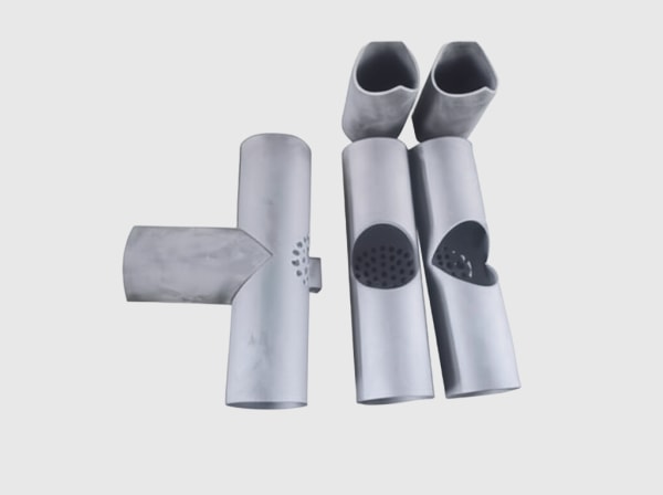
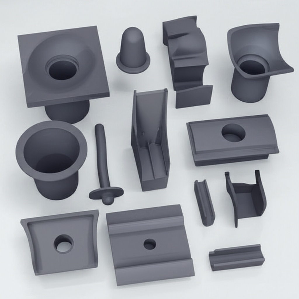
Design and Manufacturing Considerations for Nano SiC Components
Working with nano silicon carbide to create functional components presents unique design and manufacturing challenges compared to conventional materials or even micro-scale SiC. Engineers and manufacturers must consider the specific behaviors of nanomaterials throughout the production lifecycle.
Key Design Considerations:
- Material Form Selection: Decide whether the application requires bulk nano-sintered SiC, a nano SiC coating, or a nano SiC-reinforced composite. This primary choice dictates subsequent design and manufacturing strategies.
- Component Geometry and Complexity:
- Shrinkage: Nano SiC powders exhibit significant shrinkage during sintering (often 15-25%). This must be accurately factored into the initial (“green” body) design to achieve final desired dimensions.
- Wall Thickness and Aspect Ratios: Very thin walls or high aspect ratios can be challenging to produce without defects due to differential sintering or stress concentrations. Design for manufacturability (DfM) principles are crucial.
- Internal Features: Complex internal geometries may require advanced forming techniques like additive manufacturing (still emerging for SiC) or sacrificial tooling.
- Stress Distribution and Management:
- While nano SiC can offer improved toughness, it is still a ceramic and thus inherently brittle. Designs should aim to minimize stress concentrators like sharp corners or abrupt changes in thickness. Finite Element Analysis (FEA) is often employed to predict stress distributions under operational loads.
- Joining and Assembly: If the nano SiC component needs to be joined to other parts (SiC or other materials), the joining method (e.g., brazing, diffusion bonding, adhesive bonding) and interface design are critical. Coefficients of thermal expansion (CTE) mismatch must be managed.
Manufacturing Process Considerations:
- Powder Handling and Processing:
- Agglomeration: Nanoparticles have a strong tendency to agglomerate due to high surface energy. Effective de-agglomeration and dispersion techniques (e.g., high-energy milling, use of dispersants) are vital for achieving a uniform green body and, consequently, a dense, homogenous sintered part.
- Homogeneity: Ensuring uniform distribution of nano SiC particles, sintering aids (if any), and binders in the green body is essential for consistent final properties.
- Safety: Handling nanopowders requires appropriate safety measures, including respiratory protection and containment, to mitigate potential health risks.
- Forming Techniques:
- Pressing (Uniaxial, Isostatic): Common for simpler shapes. Achieving uniform density in the green body can be challenging with nanopowders.
- Slip Casting and Tape Casting: Require stable, well-dispersed nano SiC slurries.
- Injection Molding (Ceramic Injection Molding – CIM): Suitable for complex, net-shape parts but requires careful binder selection and debinding processes.
- Extrusion: For producing rods, tubes, and other constant cross-section profiles.
- Additive Manufacturing (e.g., Binder Jetting, Stereolithography): Emerging technologies for creating highly complex nano SiC parts with greater design freedom, though still under development for widespread industrial use.
- Sintering:
- Sintering Atmosphere: Typically inert (e.g., Argon) or vacuum to prevent oxidation.
- Temperature and Pressure: Nano SiC can sometimes be sintered at lower temperatures than micro-SiC, but specialized techniques like Spark Plasma Sintering (SPS) or Hot Isostatic Pressing (HIP) may be used to achieve high densities and fine microstructures.
- Sintering Aids: Additives (e.g., boron, carbon, alumina, yttria) are often necessary to promote densification of covalent materials like SiC. The choice and amount of sintering aid can affect final properties.
- Green Machining vs. Hard Machining: Machining in the “green” state (before full sintering) is easier but less precise. Machining fully sintered nano SiC is very difficult due to its extreme hardness and requires diamond tooling and specialized grinding/lapping processes.
Successfully manufacturing custom nano SiC components requires a deep understanding of materials science, ceramic processing, and precision engineering. Close collaboration between designers, material scientists, and manufacturing engineers is essential.
Achieving Precision: Tolerance, Surface Finish, and Dimensional Control with Nano SiC
For many advanced applications, particularly in semiconductors, optics, and precision machinery, the dimensional accuracy, achievable tolerances, and surface finish of nano silicon carbide components are paramount. The unique characteristics of nano SiC, while offering property enhancements, also influence these aspects.
Dimensional Tolerances:
Achieving tight dimensional tolerances with sintered nano SiC parts is challenging but possible with careful process control.
- As-Sintered Tolerances: Due to the significant and somewhat variable shrinkage during sintering, as-sintered tolerances are typically wider. For small, simple parts, tolerances in the range of ±0.5% to ±2% of the dimension might be achievable, but this depends heavily on the complexity, size, and consistency of the powder and forming process.
- Machined Tolerances: For tighter tolerances, post-sintering machining (grinding, lapping) is almost always necessary. Using advanced diamond grinding techniques, it’s possible to achieve:
- General machined tolerances: ±0.025 mm to ±0.050 mm (±0.001″ to ±0.002″).
- Precision machined tolerances: Down to ±0.005 mm to ±0.010 mm (±0.0002″ to ±0.0004″) for critical dimensions on smaller parts.
- Ultra-precision machining: In some specialized applications, even tighter tolerances approaching ±0.001 mm (±0.00004″) can be met, but this incurs significant cost and requires specialized equipment and expertise.
- Influence of Nanostructure: The fine-grained microstructure resulting from nano SiC powders can lead to more uniform material removal during machining, potentially aiding in achieving tighter tolerances compared to coarser-grained SiC.
Surface Finish:
The surface finish of nano SiC components can be tailored to application requirements, ranging from a standard machined finish to a super-polished optical surface.
- As-Sintered Surface: The surface finish of as-sintered parts is generally rough, reflecting the particle size and forming method. It’s typically not suitable for applications requiring smooth surfaces.
- Ground Surface: Grinding with diamond wheels can achieve surface roughness (Ra) values typically in the range of 0.2 µm to 0.8 µm (8 µin to 32 µin).
- Lapped Surface: Lapping with progressively finer diamond abrasives can significantly improve surface finish, achieving Ra values from 0.05 µm to 0.2 µm (2 µin to 8 µin).
- Polished Surface: For optical or ultra-smooth requirements (e.g., semiconductor wafer chucks, mirrors), nano SiC can be polished to an Ra of less than 0.01 µm to 0.025 µm (0.4 µin to 1 µin), and in some cases, even down to Angstrom-level smoothness. The fine, homogenous microstructure of nano-sintered SiC is advantageous for achieving such super-smooth, defect-free surfaces.
- Coatings: For nano SiC coatings, the surface finish is highly dependent on the deposition technique and parameters. Some CVD processes can produce very smooth films.
Dimensional Control Factors:
Maintaining consistent dimensional control throughout the manufacturing process is critical. Key factors include:
- Powder Quality: Consistent nano SiC powder characteristics (particle size, distribution, purity, surface chemistry) are foundational.
- Green Body Formation: Uniform density and homogeneity in the green body minimize warpage and differential shrinkage during sintering. Precise tooling and controlled forming parameters are essential.
- Sintering Process Control: Accurate control of sintering temperature profiles, atmosphere, and pressure (if applicable) is vital for predictable shrinkage and densification.
- Machining Expertise: Skilled operators and appropriate diamond tooling/equipment are necessary for precision machining of hard SiC. Fixturing and minimizing machining stresses are also important.
- Metrology and Inspection: Advanced metrology tools (CMMs, optical profilometers, interferometers) are required to verify dimensions and surface finish.
Procurement managers should discuss their specific tolerance and surface finish requirements with experienced SiC manufacturers who can advise on feasibility and cost implications. The use of nano SiC can facilitate finer surface finishes and potentially more intricate details due to the refined microstructure it enables.
Post-Processing Needs for Enhanced Nano SiC Performance and Durability
While nano silicon carbide intrinsically offers superior properties, many applications benefit from or require specific post-processing steps after initial forming and sintering. These treatments aim to further enhance performance, meet stringent specifications, or prepare components for assembly and final use.
Common Post-Processing Techniques:
- Precision Grinding and Lapping:
- Purpose: To achieve tight dimensional tolerances, specific geometric forms (flatness, parallelism, roundness), and desired surface finishes. Given the extreme hardness of sintered nano SiC, diamond abrasives are exclusively used.
- Process: Involves removing material using bonded diamond grinding wheels or free abrasives in a lapping slurry. Progressively finer abrasives are used to improve surface quality.
- Considerations: Can be time-consuming and costly, especially for complex geometries or ultra-fine finishes. Heat generation and subsurface damage must be carefully controlled.
- Polishing:
- Purpose: To create extremely smooth, often mirror-like surfaces, primarily for optical applications, semiconductor handling equipment (e.g., ESCs, wafer chucks), or where minimal friction is required.
- Process: Typically follows grinding and lapping, using very fine diamond slurries or chemical-mechanical polishing (CMP) techniques. CMP combines chemical action with mechanical abrasion for superior smoothness and minimal subsurface damage.
- Benefit of Nano SiC: The fine, uniform microstructure of well-processed nano SiC can be polished to a higher degree of perfection with fewer surface defects compared to coarser-grained SiC.
- Cleaning and Surface Treatment:
- Purpose: To remove contaminants, machining residues, or organic films from the surface. This is critical for applications in ultra-high vacuum, semiconductor processing, or medical devices.
- Methods: Ultrasonic cleaning in specialized solvents, plasma etching, or chemical etching. Surface passivation might also be performed to enhance chemical resistance or alter surface energy.
- Annealing or Heat Treatment:
- Purpose: To relieve internal stresses induced during machining or sintering, to further stabilize the microstructure, or to modify specific physical properties.
- Process: Controlled heating and cooling cycles in a specific atmosphere.
- Coating Application (on Nano SiC or by Nano SiC):
- Purpose:
- Applying a functional coating (e.g., metallic for brazing, dielectric for insulation) onto a nano SiC component.
- Using nano SiC as a coating material itself (e.g., CVD SiC, PVD SiC) on other substrates for wear or corrosion resistance.
- Methods: PVD, CVD, thermal spray, sol-gel, depending on the coating material and desired properties.
- Purpose:
- Edge Profiling and Chamfering:
- Purpose: To remove sharp edges, which can be sources of stress concentration and crack initiation in brittle ceramics. Chamfered or rounded edges also improve handling safety and can be critical for fit and assembly.
- Process: Specialized grinding or lapping operations.
- Joining and Assembly Pre-Treatments:
- Purpose: If the nano SiC part is to be brazed or bonded, surfaces may require metallization (e.g., sputtering Ti/Ni/Ag layers) to promote wetting and adhesion of the joining material.
- Sealing (for Porous Grades):
- Purpose: While fully dense nano SiC is ideal, some forms like reaction-bonded SiC (often containing nano-scale SiC phases) might have residual porosity. Sealing with glass, resin, or via chemical vapor infiltration (CVI) of SiC can improve gas tightness and chemical resistance.
- Note: True nano-sintered SiC, when processed correctly, aims for near-full density, minimizing the need for sealing.
The extent and type of post-processing are highly dependent on the end-use of the nano SiC component. Technical buyers should clearly specify all post-processing requirements to ensure the supplied parts meet all functional and quality criteria. Each step adds to the overall co

About the Author: Sicarb Tech
We provide clear and reliable insights into silicon carbide materials, component manufacturing, application technologies, and global market trends. Our content reflects industry expertise, practical experience, and a commitment to helping readers understand the evolving SiC landscape.

Customizable SiC
You May Also Interest
-
![]()
Mastering Extreme Conditions: Why Custom Silicon Carbide is Revolutionizing Fluid Handling
In the demanding world of industrial fluid handling, equipment is constantly under siege from corrosive chemicals, abrasive slurries, high temperatures, and extreme pressures. Traditional materials often fall short, leading to frequent downtime, costly maintenance, and compromised operational efficiency. Enter custom silicon carbide (SiC), a high-performance technical ceramic that is rapidly becoming the material of choice…
-
![]()
Europe’s Leading SiC Distributors for Easy Supply
Europe’s Leading SiC Distributors for Easy Supply In the rapidly evolving landscape of advanced materials, Silicon Carbide (SiC) stands out as a game-changer. Its unparalleled properties make it indispensable across a spectrum of high-performance industrial applications. For engineers, procurement managers, and technical buyers in industries ranging from semiconductors and automotive to aerospace and renewable energy,…
-
![]()
Silicon Carbide for Filtration: Revolutionizing Separation in Demanding Environments
In the ever-evolving landscape of industrial processing, the demand for highly efficient, durable, and reliable filtration solutions has never been greater. As industries push the boundaries of temperature, pressure, and chemical aggression, conventional filter materials often fall short. This is where custom silicon carbide (SiC) filtration products emerge as a game-changing technology. Renowned for their…