Silicon Carbide: Powering the Next Generation of High-Efficiency Electronics
Share
The demand for more efficient, compact, and robust power electronics is skyrocketing across industries, from electric vehicles and renewable energy systems to advanced industrial automation and aerospace applications. Traditional silicon-based power devices are increasingly hitting their performance limits. Enter Silicon Carbide (SiC), a wide-bandgap semiconductor material that is not just an incremental improvement but a revolutionary leap forward, enabling unprecedented levels of power density, efficiency, and high-temperature operation. For engineers, procurement managers, and technical buyers seeking a competitive edge, understanding and leveraging custom SiC solutions is no longer optional—it’s essential. This blog delves into the world of SiC for power devices, exploring its applications, advantages, and how to navigate the path to successful implementation with the right partners.
Introduction: Silicon Carbide – Revolutionizing Power Electronics
Silicon Carbide (SiC) is a compound semiconductor composed of silicon (Si) and carbon (C). Its unique physical and electrical properties make it exceptionally well-suited for power electronic devices. Unlike traditional silicon, SiC boasts a significantly wider bandgap energy (approximately 3.2 eV for 4H-SiC, a common polytype, compared to 1.1 eV for silicon). This fundamental difference translates into several key advantages:
- Higher Breakdown Electric Field: SiC can withstand much stronger electric fields before breaking down, allowing for thinner drift layers in devices. This results in lower resistive losses and enables higher blocking voltages in more compact device structures.
- Higher Thermal Conductivity: SiC is excellent at dissipating heat, a critical factor in power devices where thermal management is paramount. This allows SiC devices to operate at higher temperatures and reduces the need for bulky cooling systems.
- Higher Saturated Electron Drift Velocity: This property allows for higher switching frequencies, leading to smaller passive components (inductors and capacitors) in power conversion systems, thereby reducing overall system size, weight, and cost.
Essentially, SiC power devices, such as SiC MOSFETs (Metal-Oxide-Semiconductor Field-Effect Transistors) and SiC Schottky Diodes, can handle more power, switch faster, operate at higher temperatures, and waste less energy than their silicon counterparts. These capabilities are crucial for developing next-generation power systems that are more efficient, power-dense, and reliable. The transition to SiC is not just an upgrade; it’s a paradigm shift enabling innovation in numerous high-performance industrial applications. Companies seeking custom silicon carbide components are finding that tailored solutions can unlock even greater performance benefits.
The Unmatched Advantages of SiC in High-Power Systems
The adoption of SiC in power electronics is driven by a compelling set of advantages that directly address the shortcomings of conventional silicon technology, particularly in high-power and high-temperature environments. These benefits translate into tangible improvements in system-level performance, cost, and reliability.
- Enhanced Energy Efficiency: SiC devices exhibit significantly lower switching and conduction losses. For instance, SiC MOSFETs have much lower on-resistance (RDS(on)) per unit area and faster switching speeds with reduced energy loss during transitions compared to silicon IGBTs or MOSFETs. This leads to substantial energy savings over the operational lifetime of the equipment, a critical factor for applications like electric vehicle (EV) chargers, solar power inverters, and industrial motor drives.
- Higher Operating Temperatures: The wide bandgap and high thermal conductivity of SiC allow devices to reliably operate at junction temperatures exceeding 200∘C, and in some cases, specialized SiC devices can operate at even higher temperatures. This reduces the complexity and cost of thermal management systems, enabling more compact designs and operation in harsh environments where silicon devices would fail. This is particularly beneficial for aerospace power systems and downhole drilling applications.
- Increased Power Density: Because SiC devices can handle higher voltages and currents in smaller chip sizes, and can switch faster (reducing the size of associated passive components), the overall power density of the system can be dramatically increased. This means more power can be processed in a smaller and lighter package, a crucial advantage for applications where space and weight are at a premium, such as on-board EV chargers and portable power units.
- Higher Switching Frequencies: SiC devices can switch at frequencies several times higher than silicon devices (hundreds of kilohertz to megahertz range). This capability allows for the use of smaller inductors, capacitors, and transformers in power converters, leading to a significant reduction in the overall size, weight, and cost of the power electronics system. This is a key enabler for compact switch-mode power supplies (SMPS) and high-frequency power converters.
- Superior Reliability: The inherent material robustness of SiC contributes to a longer operational lifespan and greater stability under demanding conditions, including high temperatures and radiation environments. While early SiC devices faced some reliability challenges, advancements in material quality, device design, and manufacturing processes have led to highly reliable commercial SiC power modules.
The table below summarizes the key property comparisons between Silicon (Si) and 4H-Silicon Carbide (4H-SiC), highlighting why SiC is the superior material for demanding power applications:
| Property | Silicon (Si) | 4H-Silicon Carbide (4H-SiC) | Implication for Power Devices |
|---|---|---|---|
| Bandgap Energy (Eg) | ≈1.1 eV | ≈3.2 eV | Higher operating temperature, lower leakage current |
| Breakdown Electric Field | ≈0.3 MV/cm | ≈2−3 MV/cm (or higher) | Higher blocking voltage, thinner drift regions, lower RDS(on) |
| Thermal Conductivity | ≈1.5 W/cm-K | ≈3−5 W/cm-K | Better heat dissipation, higher current capability |
| Saturated Electron Drift Velocity | ≈1×107 cm/s | ≈2×107 cm/s | Higher switching frequency |
These advantages collectively position SiC as a cornerstone technology for the future of power electronics, enabling innovation and efficiency gains across a wide spectrum of industrial applications.
Transformative Applications: Where SiC Power Devices Shine
The unique properties of Silicon Carbide power devices are unlocking new levels of performance and efficiency in a diverse range of demanding applications. Industries are increasingly turning to custom SiC solutions to meet stringent requirements for power density, thermal management, and energy conservation.
Electric Vehicles (EVs) and Transportation: This is arguably the most visible and rapidly growing application for SiC power devices.
- Traction Inverters: SiC inverters convert DC power from the battery to AC power for the motor with significantly higher efficiency than silicon IGBTs. This translates to increased vehicle range, reduced battery size, or improved performance.
- On-Board Chargers (OBCs): SiC-based OBCs can be smaller, lighter, and more efficient, allowing for faster charging times and easier integration into the vehicle.
- DC-DC Converters: For stepping up or down voltage levels within the EV’s power distribution system, SiC converters offer higher efficiency and power density.
- Fast Charging Infrastructure: SiC is crucial for high-power off-board DC fast chargers, enabling rapid charging cycles by handling higher voltages and currents efficiently.
Renewable Energy Systems: The efficiency and reliability of SiC are vital for maximizing energy harvest and grid integration.
- Solar Power Inverters: SiC inverters improve the efficiency of converting DC power generated by solar panels to AC power for the grid or local use. Their higher switching frequencies also allow for smaller and lighter inverter designs.
- Wind Turbine Converters: In wind power systems, SiC-based converters offer enhanced efficiency and reliability in converting the variable frequency output of wind turbines to grid-compatible AC power.
- Energy Storage Systems: SiC power conversion systems (PCS) for battery energy storage offer higher round-trip efficiency and faster response times.
Industrial Power and Motor Drives: Improving energy efficiency in industrial settings is a major driver for SiC adoption.
- Variable Frequency Drives (VFDs): SiC-based VFDs for industrial motors can significantly reduce energy consumption, especially in applications with variable loads.
- Uninterruptible Power Supplies (UPS): SiC technology leads to more compact and efficient UPS systems, critical for data centers, medical facilities, and industrial processes.
- Welding Equipment and Industrial Heating: The high power and frequency capabilities of SiC are beneficial in these demanding applications.
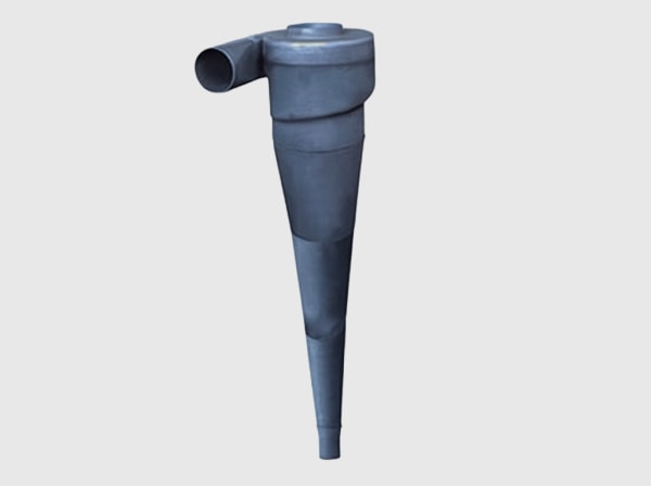
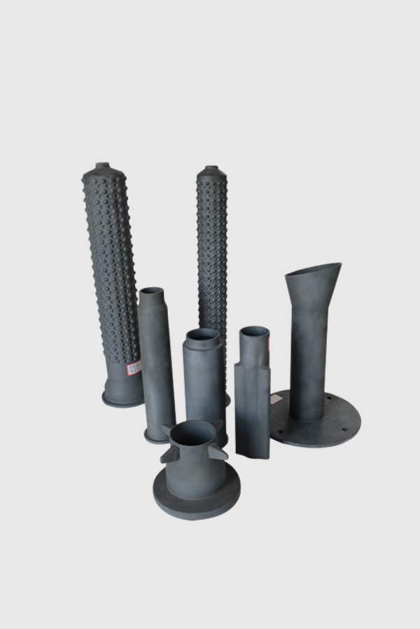
- High-Temperature Furnaces: Beyond the devices themselves, SiC ceramics like reaction-bonded silicon carbide (RBSiC) and sintered silicon carbide (SSiC) are used for components within high-temperature processing equipment, showcasing the material’s versatility. Companies requiring custom SiC heating elements or SiC furnace linings benefit from its thermal stability.
Power Supplies and Data Centers: The relentless demand for more data processing power requires highly efficient and dense power delivery.
- Server Power Supplies: SiC in power supplies for servers and telecom equipment reduces energy consumption and heat generation, lowering operational costs for data centers.
- Telecommunication Power: Compact and efficient SiC rectifiers and converters are essential for 5G infrastructure and other telecom applications.
Aerospace and Defense: The need for lightweight, reliable, and high-temperature capable electronics makes SiC a natural fit.
- Actuation Systems: SiC power modules can drive electric actuators in aircraft more efficiently.
- Radar Systems: High-power, high-frequency SiC devices are enabling more powerful and compact radar systems.
- Power Distribution in Aircraft and Satellites: The weight and size reduction offered by SiC is invaluable in these applications.
The breadth of these applications underscores the transformative impact of SiC power electronics. As the technology matures and costs decrease, its penetration into even more sectors is inevitable, making the search for reliable wholesale SiC power modules and OEM SiC solutions increasingly common.
Key SiC Materials and Structures for Power Devices
The exceptional performance of SiC power devices stems from the intrinsic properties of the silicon carbide material itself and the sophisticated device structures developed to harness these properties. Understanding the foundational material aspects is crucial for appreciating the technology and for making informed decisions when specifying custom SiC components for power applications.
Silicon Carbide Polytypes: Silicon carbide can exist in many different crystal structures known as polytypes. While over 250 polytypes have been identified, a few are dominant in semiconductor applications:
- 4H-SiC: This is the most widely used polytype for power devices due to its superior combination of high electron mobility, high breakdown field, and good thermal conductivity. The “4H” refers to the stacking sequence of atomic layers in its hexagonal crystal structure. Most commercial SiC MOSFETs and SiC Schottky Barrier Diodes (SBDs) are fabricated on 4H-SiC substrates.
- 6H-SiC: This was one of the earlier polytypes to be developed but has largely been superseded by 4H-SiC for most power device applications due to 4H-SiC’s better electron mobility, especially in the direction perpendicular to the basal plane, which is critical for vertical power device structures.
- 3C-SiC (Cubic SiC): This polytype has a potentially higher electron mobility and can be grown on silicon substrates, offering a cost advantage. However, it suffers from a lower breakdown field and more challenging defect control compared to 4H-SiC, limiting its current commercial use in high-power devices, though research continues.
SiC Substrates and Epitaxial Layers: The foundation of a SiC power device is the substrate, which is a single crystal wafer of SiC.
- SiC Substrates: High-quality, low-defect SiC substrates (typically 4H-SiC) are produced through a complex crystal growth process, often a modified Lely method or Physical Vapor Transport (PVT). The diameter of these wafers has been increasing, with 150mm (6-inch) wafers being common and 200mm (8-inch) wafers becoming more available, which helps reduce device manufacturing costs. The quality of the substrate, particularly its defect density (e.g., micropipes, dislocations), is critical for the yield and reliability of the final devices.
- SiC Epitaxial Layers: On top of the SiC substrate, one or more thin, precisely controlled layers of SiC, known as epitaxial layers (or epi-layers), are grown. These layers, typically created via Chemical Vapor Deposition (CVD), form the active regions of the power device. The thickness, doping concentration, and uniformity of these epi-layers are crucial for determining the device’s voltage rating, on-resistance, and other electrical characteristics. Advanced SiC materials technology for epitaxy is a key area of expertise.
Common SiC Power Device Structures:
- SiC Schottky Barrier Diodes (SBDs): These are typically the first SiC devices to gain widespread commercial adoption. They offer near-zero reverse recovery charge, which significantly reduces switching losses in systems where they are used as freewheeling diodes alongside transistors. Their performance is much superior to silicon PiN diodes in high-frequency applications.
- SiC MOSFETs: These are rapidly becoming the device of choice for high-performance switching applications. SiC MOSFETs offer low on-resistance, high blocking voltage, fast switching speeds, and high-temperature operation. They are replacing silicon IGBTs and MOSFETs in many applications. The quality of the gate oxide (typically SiO2 on SiC) and the interface between the oxide and the SiC is a critical aspect of SiC MOSFET technology, impacting device reliability and channel mobility.
- SiC Junction Gate Field-Effect Transistors (JFETs): These are robust devices that can operate at very high temperatures. They are typically “normally-on” devices, though normally-off variants exist.
- SiC Bipolar Junction Transistors (BJTs): While less common than MOSFETs or JFETs, SiC BJTs can offer very low on-resistance for high-current applications.
For procurement professionals and OEMs, understanding these material and device fundamentals helps in specifying the right technical ceramics for electronics and engaging effectively with SiC component suppliers. Companies like Sicarb Tech, with their deep understanding of material science and processing, play a vital role in providing the high-quality SiC materials and custom SiC fabrication support needed for these advanced power devices. Their roots in Weifang, a major hub for SiC production in China, and their collaboration with the Chinese Academy of Sciences give them a unique perspective on the entire SiC value chain.
Critical Design and Manufacturing Considerations for SiC Power Devices
The development and fabrication of reliable, high-performance Silicon Carbide power devices involve a series of intricate design and manufacturing steps, each with its own set of challenges and critical parameters. While SiC offers substantial theoretical advantages, realizing these in practical devices requires sophisticated expertise in materials science, semiconductor physics, and process engineering. Custom SiC power components demand meticulous attention to these details.
Device Design and Simulation:
- Electric Field Management: A key aspect of SiC device design is managing the high electric fields to prevent premature breakdown. This involves optimizing termination structures (like Junction Termination Extensions or guard rings) and field plate designs.
- Thermal Design: While SiC operates at high temperatures, effective thermal management at the device and package level is still crucial to ensure reliability and performance. This includes minimizing thermal resistance from the SiC chip to the heat sink.
- Gate Oxide Reliability (for MOSFETs): The interface between the gate oxide (SiO2) and the SiC material is a critical area. Ensuring long-term reliability of the gate oxide under high electric fields and temperatures is a major focus. This involves optimizing oxidation processes and post-oxidation treatments.
- Channel Mobility (for MOSFETs): The electron mobility in the inversion channel of a SiC MOSFET can be lower than in bulk SiC due to interface states and scattering mechanisms. Device designs and fabrication processes aim to maximize this mobility to achieve low on-resistance.
Wafer Processing and Fabrication: SiC wafer processing shares some similarities with silicon processing but also has unique challenges due to SiC’s hardness and chemical inertness.
- Substrate and Epitaxy Quality: As mentioned earlier, the starting material quality is paramount. Low defect density in both the SiC substrate and the epitaxial layers is essential for high device yield and reliability. This is a key focus for SiC foundry services.
- Ion Implantation and Annealing: Doping SiC to create p-type and n-type regions is typically done by ion implantation. Due to SiC’s stability, implanted dopants require very high-temperature annealing (often >1600∘C) to activate them and repair crystal damage, which is a technologically demanding step.
- Etching: SiC is highly resistant to wet chemical etching. Plasma etching (dry etching) techniques are predominantly used, requiring specialized equipment and process optimization to achieve desired profiles and selectivity.
- Metallization: Forming low-resistance ohmic contacts to both n-type and p-type SiC is crucial for device performance. This involves specific metal schemes and high-temperature annealing. Nickel-based contacts are common for n-type SiC, while aluminum-titanium alloys are often used for p-type SiC.
- Passivation: Surface passivation layers are applied to protect the device and ensure long-term stability.
Achieving High Yields and Quality Control: Manufacturing SiC devices with consistently high yields is more challenging than with silicon due to the higher defect densities in SiC wafers and the more complex processing steps.
- Defect Control: Minimizing and mitigating the impact of crystallographic defects (micropipes, stacking faults, dislocations) throughout the manufacturing process is critical.
- Process Control: Tight control over all fabrication steps, including epitaxy, implantation, etching, and metallization, is necessary to achieve the desired device parameters uniformly across the wafer.
- Testing and Characterization: Rigorous on-wafer and packaged device testing is essential to screen out faulty devices and ensure that performance specifications are met. This includes static and dynamic electrical testing, as well as reliability testing under various stress conditions (e.g., High-Temperature Reverse Bias – HTRB).
The complexity of these processes means that successful SiC device manufacturing relies on specialized knowledge and equipment. Companies looking for custom SiC fabrication or seeking to establish their own production capabilities must consider these challenges. This is where organizations like Sicarb Tech can provide immense value, not only through the supply of high-quality SiC materials or components for manufacturing equipment but also through their technology transfer services for professional silicon carbide production. Their expertise, backed by the Chinese Academy of Sciences National Technology Transfer Center, can help enterprises navigate the complexities of setting up and optimizing SiC production lines.
The following table outlines common manufacturing stages and associated considerations for SiC power devices:
| Manufacturing Stage | Key Process Steps | Critical Considerations |
|---|---|---|
| Material Preparation | Substrate growth, Epitaxial layer deposition | Defect density (micropipes, dislocations), layer thickness & doping uniformity, surface morphology |
| Device Fabrication | Ion implantation, High-temperature annealing, Etching, Lithography, Gate oxide formation (MOSFETs), Metallization, Passivation | Dopant activation, etch profile control, oxide quality, contact resistance, process uniformity, yield |
| Testing & Packaging | Wafer-level testing, Dicing, Die attach, Wire bonding, Encapsulation, Final testing | Electrical parameter verification, thermal management in package, reliability under stress |
Understanding these manufacturing intricacies helps technical buyers and engineers appreciate the value and complexity behind high-performance SiC power modules and underscores the importance of selecting partners with proven capabilities in advanced SiC materials and fabrication.
Navigating Challenges in SiC Device Fabrication and Implementation
While Silicon Carbide offers transformative potential for power electronics, its journey from raw material to a fully operational device in a system is not without its hurdles. Both manufacturers and end-users face specific challenges that need to be addressed to fully unlock the benefits of SiC technology. These range from material imperfections to system-level integration complexities.
Material-Related Challenges:
- Defect Density in Substrates and Epi-layers: Despite significant progress, SiC wafers still have higher densities of crystallographic defects (e.g., micropipes, basal plane dislocations, stacking faults) compared to silicon wafers. These defects can impair device performance, yield, and long-term reliability. Micropipes, for instance, can cause premature breakdown. Basal plane dislocations in the drift layer of bipolar devices like PiN diodes can lead to an increase in forward voltage over time (bipolar degradation). Continuous improvement in SiC crystal growth and epitaxy techniques is crucial.
- Cost of SiC Wafers: SiC substrates are currently more expensive than silicon substrates, primarily due to the complex and energy-intensive crystal growth process and lower production volumes. While costs are decreasing with larger wafer diameters (150mm and 200mm) and improved manufacturing efficiencies, the initial material cost remains a factor in the overall price of SiC power devices.
- Wafer Bow and Warp: Scaling to larger diameter SiC wafers can introduce challenges in maintaining wafer flatness, which can affect lithography and other processing steps.
Device Fabrication Challenges:
- Gate Oxide Reliability in SiC MOSFETs: The interface between the silicon dioxide (SiO2) gate dielectric and the SiC semiconductor is a critical area for MOSFETs. Threshold voltage instability and premature breakdown of the gate oxide have been historical concerns. Significant research has gone into optimizing oxidation processes (e.g., using nitric oxide or nitrous oxide anneals) to improve interface quality and long-term reliability. However, it remains an area of active development and stringent qualification for commercial SiC power modules.
- Low Channel Mobility: The electron mobility in the inversion channel of SiC MOSFETs, particularly at the SiO2/SiC interface, can be limited by interface traps and scattering mechanisms. This directly impacts the on-resistance of the device. Various surface treatments and gate dielectric materials are being explored to enhance channel mobility.
- Doping and Activation: As mentioned, activating implanted dopants in SiC requires very high temperatures, which can be challenging for process integration and can also lead to surface roughening if not carefully controlled.
- Processing Robustness: The hardness and chemical inertness of SiC make processes like etching and chemical-mechanical planarization (CMP) more difficult and costly than for silicon.
System Implementation and Packaging Challenges:
- Driving SiC Devices: SiC MOSFETs often require specific gate driver considerations, including appropriate gate voltage levels (sometimes negative turn-off voltages) and fast slew rates to take full advantage of their high-speed switching capabilities. This may necessitate more advanced gate driver ICs.
- Managing EMI: The fast switching speeds of SiC devices, while beneficial for efficiency and system size, can lead to increased electromagnetic interference (EMI). Careful PCB layout, shielding, and filtering techniques are essential.
- Thermal Management at the Package Level: While SiC chips can operate at high temperatures, the packaging materials and thermal interfaces must also be able to withstand these conditions and efficiently dissipate heat. Advanced packaging solutions with low thermal resistance and high reliability are needed, especially for high-power SiC components.
- Cost of SiC Devices and Modules: While system-level benefits (smaller passives, reduced cooling) can offset the higher device cost, the upfront component cost of SiC devices is still generally higher than their silicon counterparts. This price differential is narrowing but remains a consideration for wholesale SiC power modules and OEM SiC solutions procurement.
- Reliability and Lifetime Prediction: As a newer technology compared to silicon, long-term reliability data for SiC devices in diverse applications is still being accumulated. Developing accurate lifetime prediction models under various operational stresses is crucial for mission-critical applications.
Overcoming these challenges requires a concerted effort from material suppliers, device manufacturers, and system designers. Investment in research and development, advancements in manufacturing technology, and the development of industry standards are all contributing to the maturation of the SiC ecosystem. For companies considering adopting SiC, partnering with experienced suppliers who understand these challenges and can provide robust solutions and technical support is vital. Sicarb Tech, through its deep material expertise and connections within the Weifang SiC industrial cluster, is well-positioned to assist clients in navigating the complexities of SiC materials and their applications, offering both high-quality custom silicon carbide products and valuable insights into manufacturing best practices.
Choosing Your Strategic Partner for Custom SiC Solutions: The SicSino Advantage
The successful integration of Silicon Carbide power devices into your products and systems hinges significantly on the capabilities and reliability of your SiC component supplier. As the demand for custom SiC products, technical ceramics, and industrial SiC applications grows, selecting a partner that offers more than just off-the-shelf components becomes paramount. This is where Sicarb Tech emerges as a strategic ally, particularly for businesses seeking high-quality, cost-competitive solutions and deep technical expertise.
When evaluating potential SiC suppliers, procurement professionals, OEMs, and technical buyers should consider the following crucial factors:
- Technical Expertise and Material Knowledge: The supplier should possess a profound understanding of SiC materials science, including different grades (e.g., reaction-bonded SiC (RBSiC), sintered SiC (SSiC)), their properties, and their suitability for specific applications, especially in the context of power device manufacturing or related equipment components. SicSino, backed by the formidable scientific and technological capabilities of the Chinese Academy of Sciences and operating from the Chinese Academy of Sciences (Weifang) Innovation Park, boasts a domestic top-tier professional team specializing in customized SiC production.
- Customization Capabilities: Standard products may not always meet the unique requirements of advanced power systems. A supplier’s ability to provide custom SiC fabrication, including tailored geometries, specific material compositions, and integrated solutions from materials to finished products, is a significant advantage. SicSino excels here, leveraging a wide array of technologies in material, process, design, measurement, and evaluation to meet diverse customization needs.
- Quality Assurance and Certifications: Consistent quality is non-negotiable, especially for components used in high-reliability power electronics. Look for suppliers with robust quality management systems, traceability, and relevant certifications. SicSino emphasizes reliable quality and supply assurance, benefiting from its direct involvement in advancing local SiC production technologies.
- Supply Chain Reliability and Scalability: The supplier should have a stable supply chain and the capacity to scale production to meet your current and future demands. SicSino’s location in Weifang City, the heart of China’s SiC customizable parts manufacturing (accounting for over 80% of the nation’s total SiC output), provides a unique advantage. Having supported over 10 local enterprises with their technologies, SicSino demonstrates a strong foundation for reliable supply.
- Cost-Effectiveness: While quality and performance are key, cost remains an important consideration. A good supplier should offer competitive pricing without compromising on quality. SicSino is committed to offering higher-quality, cost-competitive customized silicon carbide components within China.
- Comprehensive Support and Partnership: Beyond just supplying parts, a strategic partner offers technical support, design assistance, and problem-solving capabilities. SicSino’s engagement goes further, even offering technology transfer for professional silicon carbide production. If you aim to establish your own specialized SiC products manufacturing plant, SicSino can provide turnkey project services, including factory design, equipment procurement, installation, commissioning, and trial production. This unique offering ensures a more effective investment and reliable technology transformation.
The SicSino Advantage:
Sicarb Tech is not just another supplier; it is an enabler of SiC technology. Having introduced and implemented SiC production technology since 2015, SicSino has been instrumental in the technological advancement and large-scale production capabilities of the Weifang SiC industry cluster.
| SicSino Capability | Benefit to Your Business |
|---|---|
| Deep Chinese Academy of Sciences Backing | Access to cutting-edge research, top-tier talent, and a national-level innovation platform. |
| Weifang SiC Hub Location | Proximity to a vast production base, ensuring supply chain resilience and access to a skilled workforce. |
| Proven Customization | Tailored SiC components and solutions (materials, process, design) to meet specific application needs. |
| Integrated Process Expertise | From raw materials to finished products, ensuring quality control and optimization at every stage. |
| Technology Transfer Services | Unique capability to help clients establish their own SiC manufacturing plants with full turnkey support. |
| Commitment to Quality & Cost | Delivering high-quality, cost-competitive SiC solutions. |
Choosing Sicarb Tech means partnering with an organization that is deeply embedded in the SiC industry’s core, from fundamental research to mass production. For businesses looking to leverage the power of SiC, whether through custom SiC components for power device packaging, thermal management, or specialized parts for SiC manufacturing equipment, SicSino offers a reliable and knowledgeable pathway to success. Their role as a bridge for technology transfer and commercialization, supported by the Chinese Academy of Sciences National Technology Transfer Center, underscores their commitment to advancing the entire SiC ecosystem.
Frequently Asked Questions (FAQ) about SiC Power Devices
As Silicon Carbide technology becomes more prevalent in power electronics, engineers, designers, and procurement specialists often have specific questions. Here are some common queries with concise, practical answers:
1. What are the primary advantages of SiC MOSFETs over traditional Silicon IGBTs?
SiC MOSFETs offer several key advantages over Silicon Insulated Gate Bipolar Transistors (IGBTs), particularly in high-performance applications:
- Higher Switching Speed: SiC MOSFETs can switch significantly faster, leading to lower switching losses and enabling the use of smaller passive components (inductors, capacitors), thus increasing power density.
- Lower Conduction Losses: In many operating regions, SiC MOSFETs exhibit lower on-state resistance (RDS(on)) compared to the voltage drop across an IGBT, resulting in better efficiency.
- No Tailing Current: Unlike IGBTs, SiC MOSFETs do not have a “tail current” during turn-off, which further reduces switching losses and allows for more efficient operation at high frequencies.
- Higher Operating Temperature: SiC’s material properties allow MOSFETs to operate reliably at higher junction temperatures than silicon IGBTs, simplifying thermal management.
- Better Reverse Recovery of Body Diode: While the intrinsic body diode of early SiC MOSFETs had some limitations, newer generations feature significantly improved reverse recovery characteristics, often eliminating the need for an external anti-parallel SiC Schottky diode in some applications.
These benefits translate to improved system efficiency, reduced size and weight, and better overall performance, especially in applications like EV inverters, solar converters, and high-frequency power supplies.
2. Are SiC power devices significantly more expensive than silicon-based devices?
Currently, individual SiC power devices (e.g., a SiC MOSFET chip) are generally more expensive than their silicon counterparts (e.g., a silicon MOSFET or IGBT with similar ratings). This price difference is due to several factors:
- Higher Substrate Cost: SiC wafers are more complex and costly to produce than silicon wafers.
- More Complex Manufacturing: Some SiC fabrication steps are more demanding (e.g., high-temperature annealing).
- Lower Production Volumes (Historically): Although rapidly increasing, SiC production volumes are still catching up to the massive scale of silicon manufacturing.
However, it’s crucial to consider the total system cost and lifetime operational cost, not just the individual component price. The use of SiC devices can lead to:
- Reduced size and cost of passive components (inductors, capacitors, transformers) due to higher switching frequencies.
- Simplified thermal management systems (smaller heat sinks, potentially eliminating fans) due to higher efficiency and temperature capability.
- Increased overall system efficiency, leading to lower energy consumption and operational savings over the product’s lifetime.
- Higher power density, meaning more power in a smaller, lighter package, which can be a significant value in many applications.
As SiC technology matures, wafer sizes increase (e.g., to 200mm), and manufacturing economies of scale improve, the price difference for SiC components is steadily decreasing. Many analyses show that the system-level benefits often outweigh the higher initial SiC device cost, making it a cost-effective solution in the long run for demanding applications. When sourcing wholesale SiC power modules or OEM SiC solutions, it’s important to discuss these trade-offs with knowledgeable suppliers.
3. What are the main challenges in packaging SiC power devices for high-temperature and high-power applications?
Packaging SiC power devices effectively presents unique challenges due to their ability to operate at high temperatures, high voltages, and high switching frequencies:
- Thermal Management: Efficiently extracting heat from the small SiC die is critical. Packaging materials must have high thermal conductivity and be able to withstand high operating temperatures without degradation. Die-attach materials (e.g., silver sintering, advanced solders) and substrate materials (e.g., Direct Bonded Copper on ceramic, Active Metal Brazing) are key.
- Minimizing Parasitic Inductance and Capacitance: To fully exploit the fast switching speeds of SiC devices, the package must have very low parasitic inductance and capacitance. These parasitics can cause voltage overshoots, ringing, and increased switching losses. Advanced package designs, such as those minimizing wire bond lengths or using planar interconnections, are necessary.
- Material Compatibility and Reliability: All materials within the package (die attach, wire bonds, encapsulation, substrate) must be able to withstand high temperatures, high voltages, and thermal cycling without degrading or causing failures. Coefficient of Thermal Expansion (CTE) mismatches between different materials can lead to stress and delamination.
- High Voltage Isolation: For high-voltage SiC devices, the package must provide robust electrical isolation to prevent arcing and ensure safety. This requires careful design of creepage and clearance distances and the use of high-dielectric-strength materials.
- Cost-Effectiveness: Advanced packaging solutions that meet these demanding requirements can be expensive. Balancing performance and reliability with cost is an ongoing challenge for high-power SiC components.
Addressing these challenges often involves using specialized technical ceramics, advanced interconnect technologies, and sophisticated thermal interface materials. Companies specializing in custom SiC products and packaging solutions, like Sicarb Tech with its broad material and process expertise, can offer valuable insights and components that contribute to robust and reliable SiC power modules.
Conclusion: Embracing the SiC Revolution for a More Powerful Future
The era of Silicon Carbide power electronics is undeniably upon us. The material’s inherent superiority in handling high power, high temperatures, and high switching frequencies is not just a theoretical advantage but a practical reality transforming industries from automotive and renewable energy to industrial manufacturing and beyond. For engineers striving for greater efficiency, procurement managers seeking reliable and advanced components, and technical buyers aiming to integrate cutting-edge solutions, SiC power devices offer a clear pathway to innovation and competitive advantage.
The journey to adopting SiC involves understanding its multifaceted benefits—enhanced energy efficiency, increased power density, superior thermal performance, and improved system reliability. It also means navigating the nuances of SiC material grades, device design intricacies, and manufacturing challenges. Choosing the right partner is critical in this landscape. A supplier like Sicarb Tech, with its deep roots in the Weifang SiC industrial hub, strong backing from the Chinese Academy of Sciences, and proven expertise in custom silicon carbide products and even turnkey SiC production technology transfer, can significantly de-risk the adoption process and accelerate time-to-market.
By embracing custom SiC solutions, businesses can unlock new levels of performance in their power systems, reduce energy consumption, and develop more compact and robust products. The ongoing advancements in SiC wafer technology, device fabrication, and packaging, coupled with decreasing costs, are further solidifying SiC’s role as the cornerstone of next-generation power electronics. For those ready to lead in their respective fields, the strategic integration of silicon carbide for power devices is not just an option, but a fundamental step towards a more efficient, powerful, and sustainable technological future.

About the Author: Sicarb Tech
We provide clear and reliable insights into silicon carbide materials, component manufacturing, application technologies, and global market trends. Our content reflects industry expertise, practical experience, and a commitment to helping readers understand the evolving SiC landscape.

Customizable SiC
You May Also Interest
-
![]()
SiC Research Collaboration: Opportunities Await
SiC Research Collaboration: Opportunities Await The landscape of advanced materials is continually evolving, with silicon carbide (SiC) emerging as a cornerstone for innovation across a myriad of demanding industries. Its exceptional properties—high thermal conductivity, extreme hardness, chemical inertness, and semiconductor capabilities—make it indispensable for next-generation applications. As a company specializing in custom silicon carbide products…
-
![]()
Silicon Carbide: Powering the Next Generation of Electronics
The electronics industry is in a constant state of evolution, driven by the relentless demand for smaller, faster, and more efficient devices. As traditional silicon-based electronics approach their theoretical limits, new materials are stepping in to bridge the gap and unlock unprecedented performance. Among these, silicon carbide (SiC) has emerged as a frontrunner, particularly in…
-
![]()
Innovative SiC Composites for Unique Solutions
Innovative SiC Composites for Unique Solutions In the demanding landscape of modern industry, where extreme temperatures, abrasive environments, and corrosive chemicals are the norm, standard materials often fall short. This is where innovative silicon carbide (SiC) composites emerge as a game-changer. As a leading technical content writer for a company specializing in custom SiC products,…