Silicon Carbide: Powering the Next Generation of Semiconductor Innovation
Share
The semiconductor industry is the bedrock of modern technology, fueling advancements from artificial intelligence and high-performance computing to electric vehicles and renewable energy systems. As semiconductor devices become smaller, faster, and more powerful, the demands placed on the materials used in their fabrication escalate significantly. In this relentless pursuit of performance and efficiency, custom silicon carbide (SiC) products have emerged as indispensable, offering a unique combination of properties that address the critical challenges of advanced semiconductor manufacturing. This blog post explores the multifaceted role of silicon carbide in the semiconductor landscape, guiding engineers, procurement managers, and technical buyers through its applications, advantages, and considerations for sourcing high-quality custom SiC components.
Introduction: The Semiconductor Revolution and the Imperative for Advanced Materials like SiC
The semiconductor revolution is characterized by an insatiable demand for increased processing power, higher operating frequencies, and enhanced energy efficiency. Traditional materials like silicon, while foundational, are reaching their theoretical limits in certain high-power and high-temperature applications. This is where technical ceramics, and specifically silicon carbide, step in. Silicon carbide (SiC) is a compound of silicon and carbon known for its exceptional hardness, high thermal conductivity, excellent thermal shock resistance, and superior chemical inertness.
In the context of semiconductor manufacturing, these properties are not just desirable; they are essential. Processes such as plasma etching, chemical vapor deposition (CVD), and rapid thermal processing (RTP) involve extreme temperatures, corrosive chemicals, and the need for ultra-high purity and dimensional stability. Custom SiC components, designed and manufactured to precise specifications, are crucial for ensuring the reliability, yield, and cost-effectiveness of these sophisticated operations. The ability to tailor SiC parts to specific equipment and process requirements makes custom silicon carbide solutions a cornerstone of innovation in the semiconductor industry. For OEMs and distributors looking for wholesale SiC components or industrial SiC procurement, understanding the nuances of this advanced material is key to maintaining a competitive edge.
Silicon Carbide’s Pivotal Role in Modern Semiconductor Manufacturing
Silicon carbide’s unique attributes make it an ideal material for a wide array of critical components within semiconductor fabrication equipment. Its deployment directly impacts process stability, component lifetime, and ultimately, wafer yield and quality. For semiconductor equipment manufacturers, integrating high-performance SiC ceramic parts is a strategic imperative.
Key applications include:
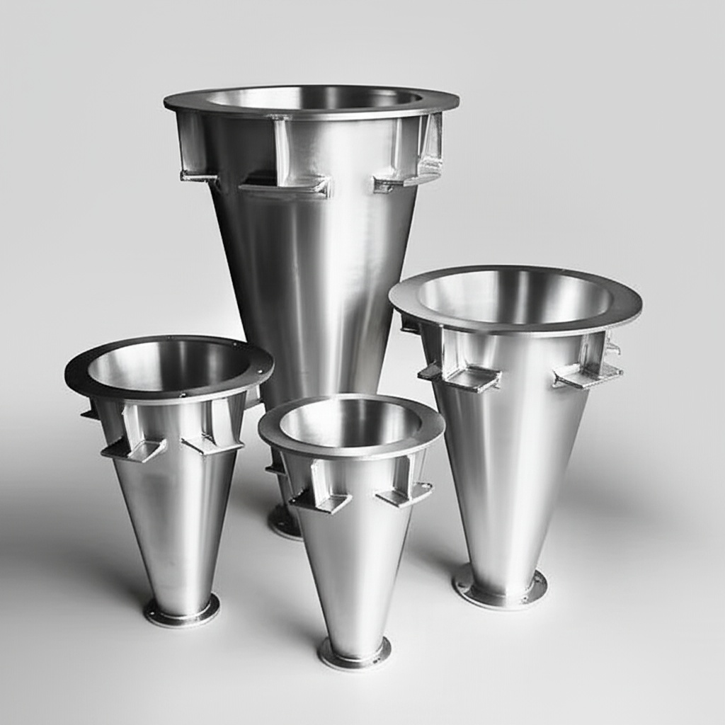
- Wafer Handling and Transfer Components: Robots and end effectors made from SiC offer high stiffness, low particle generation, and resistance to wear, crucial for safely and cleanly transporting delicate silicon wafers. SiC wafer chucks, including electrostatic chucks (E-chucks), provide uniform temperature control and secure wafer clamping during various processing steps.
- Process Chamber Components: In environments like plasma etch and CVD chambers, SiC is used for showerheads, gas distribution plates, chamber liners, edge rings, and focus rings. Its resistance to aggressive plasma chemistries and high temperatures ensures minimal contamination and extended component life. High-purity silicon carbide is particularly vital in these applications to prevent unwanted impurities from affecting the semiconductor devices.
- Thermal Processing Components: SiC’s high thermal conductivity and excellent thermal shock resistance make it suitable for susceptors, heating elements, and support structures in rapid thermal processing (RTP) systems and diffusion furnaces. These components ensure uniform temperature distribution and rapid heating/cooling cycles.
- Optics and Metrology: In some specialized applications, SiC’s optical properties and dimensional stability are leveraged for mirrors or reference blocks in metrology and inspection equipment.
- CMP (Chemical Mechanical Planarization) Rings: Retainer or guide rings in CMP processes benefit from SiC’s wear resistance and chemical stability, contributing to process consistency.
The table below highlights some common semiconductor applications and the relevant SiC properties:
| Application Area | Key SiC Components | Critical SiC Properties Benefiting Application | Target B2B Keywords for Procurement |
|---|---|---|---|
| Wafer Handling & Clamping | End Effectors, Wafer Chucks (incl. Electrostatic) | High Hardness, Wear Resistance, Thermal Conductivity, Stiffness | Custom SiC wafer chucks, SiC robotic arms |
| Plasma Etch Chambers | Showerheads, Liners, Edge Rings, Focus Rings | Chemical Inertness, Plasma Erosion Resistance, High Purity | SiC etching components, Plasma resistant SiC |
| CVD & Epitaxy Reactors | Susceptors, Gas Injectors, Chamber Liners | High Thermal Conductivity, Thermal Shock Resistance, Purity | CVD SiC components, SiC susceptors |
| Diffusion & Oxidation | Furnace Tubes, Paddles, Boats | High-Temperature Strength, Thermal Stability, Low Particle Generation | SiC furnace components, Diffusion SiC parts |
| Rapid Thermal Processing | Susceptors, Edge Rings, Support Pins | Rapid Thermal Response, High Emissivity, Thermal Uniformity | RTP SiC components, Custom thermal SiC |
This extensive use underscores the reliance of the semiconductor industry on the consistent performance of advanced ceramic materials like silicon carbide.
The Custom Silicon Carbide Advantage in Semiconductor Processes
Choosing generic, off-the-shelf components for highly sophisticated semiconductor manufacturing processes can introduce unacceptable risks and limitations. Custom silicon carbide fabrication offers distinct advantages, enabling manufacturers to optimize their equipment and processes for maximum performance, yield, and longevity. This tailored approach is essential for companies seeking bespoke SiC solutions to meet unique challenges.
The key benefits of opting for custom SiC components in semiconductor applications include:
- Optimized Thermal Management: Semiconductor processes are exquisitely sensitive to temperature variations. Custom SiC components can be designed with specific geometries and thermal properties to ensure precise temperature control across wafers, minimizing defects and improving process uniformity. This includes features like integrated cooling channels or optimized emissivity for radiative heating.
- Enhanced Wear Resistance and Longevity: The mechanical stresses and abrasive environments in wafer handling and CMP, or the erosive nature of plasma, demand materials that can withstand significant wear. Custom-designed SiC parts, potentially using specific grades like sintered SiC (SSiC) known for its extreme hardness, can lead to significantly longer component lifetimes, reducing downtime and maintenance costs for industrial manufacturing lines.
- Superior Chemical Inertness and Purity: Semiconductor fabrication involves a plethora of corrosive gases and chemicals. Custom SiC components, especially those made from high-purity grades, resist chemical attack and minimize the leaching of contaminants into the process environment. This is critical for maintaining the integrity of the delicate semiconductor devices being manufactured. Sicarb Tech and its network of manufacturers in Weifang, China, place a strong emphasis on material purity to meet these stringent semiconductor requirements.
- Precision Fit and Functionality: Generic parts may not perfectly integrate with existing equipment, leading to inefficiencies or even damage. Custom SiC components are manufactured to exact dimensional specifications, ensuring seamless integration and optimal performance within complex semiconductor tools. This precision is a hallmark of the custom SiC parts manufacturing capabilities found in leading industrial hubs.
- Design for Manufacturability (DfM): Collaborating with an experienced SiC supplier allows for DfM principles to be applied early in the design phase. This ensures that the component is not only optimized for its application but also for efficient and cost-effective manufacturing, taking into account the unique characteristics of SiC machining and forming.
Procurement managers and technical buyers focused on semiconductor-grade SiC should recognize that the initial investment in custom components often translates into lower total cost of ownership due to improved process yields, reduced maintenance, and longer equipment uptime.
Navigating SiC Grades and Compositions for Optimal Semiconductor Performance
Not all silicon carbide is created equal. Different manufacturing processes result in various SiC grades with distinct properties, making the selection of the right grade crucial for specific semiconductor applications. Understanding these differences allows engineers and technical procurement professionals to specify materials that will deliver the desired performance and reliability.
Here are some of the most common SiC grades used in or relevant to semiconductor applications:
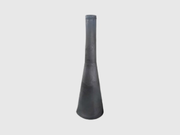
- Reaction-Bonded Silicon Carbide (RBSiC or SiSiC):
- Manufacturing: Produced by infiltrating a porous carbon preform with molten silicon. The silicon reacts with some of the carbon to form SiC, and the remaining pores are filled with silicon metal.
- Properties: Good thermal conductivity, excellent thermal shock resistance, good wear resistance, and relatively easier to produce in complex shapes. Contains free silicon (typically 8-15%), which can be a concern for ultra-high purity or certain chemical environments.
- Semiconductor Uses: Often found in larger structural components, heater elements, and some chamber furniture where extreme purity is not the absolute primary driver.
- Keywords: Reaction-bonded SiC for semiconductor, SiSiC components, Custom RBSiC parts.
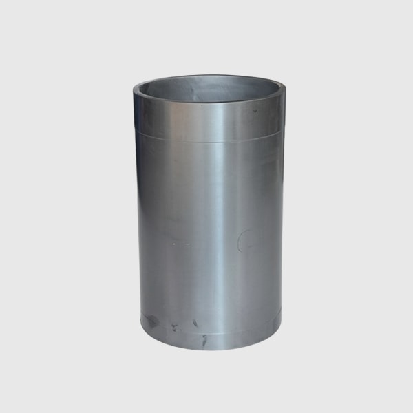
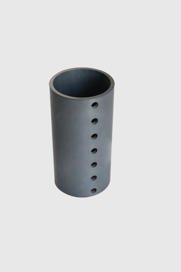
- Sintered Silicon Carbide (SSiC):
- Manufacturing: Made by sintering fine SiC powder at high temperatures (typically >2000°C), often with non-oxide sintering aids (e.g., boron and carbon). Results in a single-phase SiC material. Direct Sintered SiC (DSSiC) is a common type.
- Properties: Extremely high hardness, excellent wear resistance, high strength, good chemical inertness, and high-temperature stability. Can achieve very high purity levels.
- Semiconductor Uses: Ideal for demanding applications requiring high purity and wear resistance, such as electrostatic chucks, focus rings, edge rings, CMP rings, and precision fixtures.
- Keywords: Sintered SiC semiconductor parts, High-purity SSiC, DSSiC components.
- Nitride-Bonded Silicon Carbide (NBSiC):
- Manufacturing: SiC grains are bonded by a silicon nitride (Si3N4) phase.
- Properties: Good thermal shock resistance, good strength, and good resistance to wetting by molten metals.
- Semiconductor Uses: Less common in direct contact with wafers in ultra-clean processes compared to SSiC, but can be used for kiln furniture and fixtures in related thermal processing steps or for components where its specific bonding phase offers advantages.
- Keywords: Nitride-bonded SiC, NBSiC industrial ceramics.
- CVD Silicon Carbide (CVD-SiC):
- Manufacturing: Produced by Chemical Vapor Deposition, where gaseous precursors react to deposit a thin or thick film of highly pure SiC onto a substrate (often graphite).
- Properties: Extremely high purity (often >99.9995%), excellent chemical resistance, high stiffness, and ability to form conformal coatings or solid components.
- Semiconductor Uses: The gold standard for applications requiring the utmost purity and corrosion resistance, such as susceptors in epitaxy reactors, critical chamber components, and protective coatings on other materials.
- Keywords: CVD SiC coating, High-purity CVD SiC, Semiconductor CVD components.
The choice of SiC grade directly impacts component performance and cost. The following table provides a comparative overview:
| SiC Grade | Typical Purity | Key Advantages for Semiconductors | Common Semiconductor Applications | Relative Cost |
|---|---|---|---|---|
| RBSiC (SiSiC) | Good | Good thermal shock resistance, complex shapes, moderate cost | Heaters, structural parts, some chamber furniture | Medium |
| SSiC (Direct Sintered) | High to V. High | Excellent wear resistance, high strength, good purity, chemical inertness | E-chucks, focus/edge rings, CMP rings, precision nozzles | High |
| NBSiC | Good | Good thermal shock resistance, good strength | Kiln furniture, some specialized fixtures | Medium-High |
| CVD-SiC | Ultra-High | Highest purity, superior corrosion resistance, conformal coating ability | Epitaxy susceptors, critical etch/deposition chamber parts, SiC optics | Very High |
Precision Engineering: Design, Tolerances, and Finishing of SiC Components for Semiconductors
The performance of silicon carbide components in semiconductor manufacturing is not solely dependent on the material grade; it is equally reliant on precision engineering throughout the design, manufacturing, and finishing stages. Given SiC’s inherent hardness and brittleness, specialized expertise is required to achieve the tight tolerances and sophisticated geometries demanded by the semiconductor industry. Precision SiC machining and finishing are critical capabilities for any supplier.
Design Considerations for Manufacturability (DfM):
- Geometry Limits: While SiC can be formed into complex shapes, designers must be aware of limitations imposed by different manufacturing processes (e.g., pressing, green machining, sintering, diamond grinding). Sharp internal corners, very thin walls, or extreme aspect ratios can be challenging and costly. Early collaboration with a SiC specialist like Sicarb Tech can optimize designs for manufacturability.
- Wall Thickness: Minimum achievable wall thickness depends on the SiC grade and overall component size. It’s crucial to balance structural integrity with functional requirements like thermal mass or gas flow.
- Stress Points: SiC is a brittle ceramic, so avoiding stress concentrators like sharp notches or sudden changes in cross-section is vital. Generous radii and smooth transitions should be incorporated into the design.
- Joining and Assembly: If multiple SiC parts need to be assembled, or if SiC needs to be joined to other materials, the design must accommodate appropriate joining techniques (e.g., brazing, diffusion bonding, mechanical fastening).
Achievable Tolerances, Surface Finish & Dimensional Accuracy:
The semiconductor industry often requires dimensional tolerances in the micron range and exceptionally smooth, defect-free surfaces to prevent particle generation and ensure uniform process conditions.
- Tolerances: As-sintered SiC components typically have tolerances in the range of ±0.5% to ±2% of the dimension. However, post-sintering diamond grinding can achieve much tighter tolerances, often down to ±0.005 mm (5 microns) or even better for critical features.
- Surface Finish: Standard ground finishes for SiC can be around Ra0.4 μm to Ra0.8 μm. For applications requiring ultra-smooth surfaces, such as electrostatic chucks or mirrors, lapping and polishing techniques can achieve surface finishes well below Ra0.1 μm, sometimes even down to angstrom levels.
- Dimensional Accuracy & Stability: SiC exhibits excellent dimensional stability over a wide temperature range and is resistant to creep, ensuring that precision components maintain their critical dimensions during operation.
Post-Processing Needs:
Beyond primary shaping and grinding, several post-processing steps may be necessary to enhance the performance and durability of custom SiC semiconductor parts:
- Grinding & Lapping: As mentioned, diamond grinding is standard for achieving tight tolerances. Lapping further refines surface flatness and smoothness.
- Polishing: For optical-grade surfaces or ultra-smooth requirements on chucks, specialized polishing techniques are employed.
- Cleaning & Purity Control: Rigorous cleaning procedures are essential to remove any contaminants from machining or handling, ensuring the component meets the stringent purity requirements of semiconductor fabs. This often involves multi-stage chemical cleaning and packaging in cleanroom environments.
- Edge Chamfering/Rounding: Sharp edges can be prone to chipping and particle generation. Precise edge treatments are often required.
- Coatings (e.g., CVD-SiC): In some cases, a base SiC component (e.g., SSiC or graphite) might be coated with a layer of ultra-pure CVD-SiC to achieve the ultimate surface properties.
- Sealing: For certain porous grades of SiC or applications requiring vacuum integrity, sealing processes might be applied, though for most semiconductor applications, dense, non-porous grades like SSiC or CVD-SiC are preferred.
Technical buyers and engineers should ensure their SiC component supplier possesses advanced machining capabilities, robust metrology systems, and stringent quality control processes to deliver parts that meet exact specifications.
Overcoming Challenges in Implementing SiC Solutions for Semiconductor Applications
While silicon carbide offers substantial benefits for semiconductor applications, its adoption and implementation are not without challenges. Understanding these potential hurdles allows for proactive mitigation strategies, ensuring successful integration of SiC advanced ceramics.
Common challenges include:
- Brittleness and Machining Complexity: SiC is extremely hard, making it difficult and time-consuming to machine. This inherent brittleness also means it can be susceptible to fracture if mishandled or subjected to excessive mechanical or thermal shock beyond its design limits.
- Mitigation: Employing specialized diamond grinding techniques, experienced machinists, and careful design for manufacturability (e.g., avoiding sharp corners, ensuring proper support). Suppliers with deep expertise in ceramic machining solutions are crucial. Careful handling protocols and operator training are also essential.
- Cost: Custom SiC components, particularly high-purity grades like SSiC and CVD-SiC, can be more expensive upfront compared to traditional materials or lower-grade ceramics. This is due to raw material costs, energy-intensive processing, and complex machining.
- Mitigation: Focusing on the total cost of ownership (TCO). The extended lifespan, improved process yield, and reduced downtime offered by high-quality SiC components often offset the initial investment. Optimizing component design for efficient manufacturing and sourcing from competitive yet capable suppliers like those in the Weifang hub, facilitated by Sicarb Tech, can also help manage costs. Volume purchasing for wholesale SiC components can also provide economies of scale.
- Purity Requirements and Contamination Control: Semiconductor processes demand exceptionally high levels of purity. Any contaminants from SiC components can lead to device failure.
- Mitigation: Specifying high-purity SiC grades (e.g., SSiC, CVD-SiC). Ensuring the supplier has stringent quality control over raw materials and manufacturing processes, including cleanroom manufacturing and packaging capabilities. Requesting material certifications and contamination analysis data.
- Thermal Shock Management: While SiC generally has excellent thermal shock resistance, extreme temperature gradients or very rapid cycling beyond material limits can still pose a risk, especially for complex geometries.
- Mitigation: Proper material grade selection (RBSiC often has superior thermal shock resistance to SSiC due to its composite nature, though SSiC is generally very good). Careful component design to minimize thermal stresses. Controlled ramp-up and cool-down rates in thermal processes.
- Joining SiC to Other Materials: Creating reliable, vacuum-tight seals between SiC and other materials (like metals in an assembly) can be challenging due to differences in coefficients of thermal expansion (CTE).
- Mitigation: Utilizing specialized brazing alloys and techniques, designing CTE-matched intermediate layers, or employing mechanical clamping solutions designed to accommodate CTE mismatch. Consulting with experts in ceramic-to-metal joining.
The table below summarizes key challenges and mitigation approaches for industrial SiC procurement in the semiconductor sector:
| Challenge | Primary Impact Areas | Mitigation Strategies |
|---|---|---|
| Brittleness & Machining | Manufacturability, Handling, Cost | DfM, specialized machining, experienced suppliers, careful handling protocols. |
| Cost of High-Purity Grades | Budget Constraints | TCO analysis, design optimization, competitive sourcing (e.g., Sicarb Tech), volume considerations. |
| Purity & Contamination Control | Wafer Yield, Device Performance | Specify high-purity SiC grades, rigorous supplier QC, material certifications, cleanroom protocols. |
| Thermal Shock Susceptibility | Component Lifespan in Rapid Thermal Cycling | Appropriate grade selection (e.g. RBSiC for some applications), design for thermal stress reduction, process control (ramp rates). |
| Joining & Sealing | Assembly Integrity, Vacuum Performance | Specialized brazing, CTE management, engineered mechanical seals, expert consultation. |
Successfully navigating these challenges requires close collaboration between the end-user and a knowledgeable SiC component supplier.
Partnering for Success: Selecting Your Custom SiC Supplier for Semiconductor Components
The quality and performance of your custom silicon carbide components are directly linked to the capabilities and expertise of your chosen supplier. For procurement managers, engineers, and OEMs in the semiconductor industry, selecting the right partner for custom SiC manufacturing is a critical decision that impacts not just component quality but also supply chain reliability and overall project success.
Key factors to consider when evaluating a SiC components vendor:
- Technical Expertise and Material Knowledge: Does the supplier have a deep understanding of different SiC grades (RBSiC, SSiC, CVD-SiC, etc.) and their suitability for specific semiconductor applications? Can they provide expert advice on material selection and design optimization? Look for suppliers with a strong engineering team and a track record in technical ceramics for semiconductors.
- Manufacturing Capabilities: Assess their range of manufacturing processes (forming, sintering, green machining, precision diamond grinding, lapping, polishing). Do they have the equipment and expertise to produce complex geometries and achieve the tight tolerances and surface finishes required for semiconductor parts?
- Quality Management Systems: A robust quality management system (e.g., ISO 9001 certification) is essential. Inquire about their quality control procedures at each stage, from raw material inspection to final product verification. What metrology equipment do they use? Can they provide detailed inspection reports and material certifications?
- Purity Control and Cleanliness: For semiconductor applications, the supplier’s ability to control purity and provide components free from contamination is paramount. Do they have experience with high-purity SiC processing and cleanroom handling/packaging if required?
- Customization Capabilities and Design Support: Can the supplier work from your detailed drawings, or can they also provide design assistance and DfM (Design for Manufacturability) feedback? Flexibility and a collaborative approach are key for bespoke SiC solutions.
- Supply Chain Reliability and Lead Times: Evaluate their production capacity, typical lead times for custom orders, and their ability to manage a consistent supply chain for raw materials. Transparent communication regarding production schedules is crucial.
- Cost-Effectiveness: While cost is a factor, it should be balanced against quality, reliability, and technical support. Look for suppliers who offer good value, considering the total cost of ownership.
- Location and Support: Consider the supplier’s location for logistics and communication. However, with global shipping, expertise and capability often outweigh proximity.
This is where Sicarb Tech offers a distinct advantage. Situated in Weifang City, the hub of China’s silicon carbide customizable parts manufacturing (accounting for over 80% of the nation’s SiC output), SicSino is deeply embedded in this specialized industrial ecosystem. Since 2015, we have been instrumental in advancing SiC production technology and enabling large-scale production for local enterprises.
As part of the Chinese Academy of Sciences (Weifang) Innovation Park and backed by the national technology transfer center of the Chinese Academy of Sciences , SicSino leverages top-tier scientific, technological capabilities, and a professional team specializing in customized SiC production. We offer:
- Access to a Wide Range of Technologies: Including material, process, design, and measurement & evaluation technologies, enabling us to meet diverse customization needs for SiC OEM components.
- Quality and Cost Competitiveness: Through our network and technological support to over 10 local enterprises, we can offer higher-quality, cost-competitive custom SiC components.
- Reliable Supply Assurance: Our deep roots in the Weifang SiC cluster ensure a stable and reliable supply chain.
- Technology Transfer Services: For businesses looking to establish their own specialized SiC production, Sicarb Tech offers comprehensive technology transfer and turnkey project services, a testament to our profound expertise in SiC manufacturing from materials to finished products.
When looking for a trusted SiC parts supplier for demanding semiconductor applications, partnering with an entity like Sicarb Tech provides not just components, but a comprehensive solution grounded in innovation and extensive manufacturing experience.
Cost Drivers and Lead Time Considerations for Custom SiC Semiconductor Components:
Understanding the factors that influence pricing and delivery times is essential for effective budgeting and project planning.
- Material Grade: High-purity grades like CVD-SiC and SSiC are more expensive than RBSiC due to raw material costs and processing complexity.
- Component Complexity and Size: Intricate designs, very large or very small parts, and features requiring extensive machining will increase costs and potentially lead times.
- Tolerances and Surface Finish: Tighter tolerances and ultra-smooth surface finishes necessitate more processing steps (e.g., precision grinding, lapping, polishing), adding to cost and time.
- Order Volume: Larger production runs typically benefit from economies of scale, reducing the per-unit cost. Small, highly custom orders will have a higher unit price.
- Testing and Certification Requirements: Specialized testing (e.g., purity analysis, non-destructive testing) and detailed certification add to the overall cost and can extend lead times.
- Urgency: Expedited orders may incur additional charges.
Typical lead times for custom SiC components can range from a few weeks to several months, depending on these factors. Clear communication with your supplier from the initial inquiry stage is vital for managing expectations regarding both cost and delivery.
Frequently Asked Questions (FAQ) about SiC in Semiconductors
Q1: Why is silicon carbide preferred over other ceramics or metals for many semiconductor process chamber components? A1: Silicon carbide (especially SSiC and CVD-SiC) offers a superior combination of properties essential for semiconductor process environments. This includes excellent resistance to aggressive plasma chemistries and high temperatures, high thermal conductivity for temperature uniformity, high stiffness and wear resistance for longevity, and the ability to be produced in ultra-high purity forms to prevent wafer contamination. Metals can introduce metallic contamination and often lack the high-temperature stability or chemical resistance of SiC. Other ceramics might not offer the same balance of thermal conductivity, purity, and plasma erosion resistance.
Q2: What are the key differences between Reaction-Bonded SiC (RBSiC/SiSiC) and Sintered SiC (SSiC) for semiconductor applications? A2: The main differences lie in purity, density, and the presence of free silicon. * RBSiC/SiSiC: Contains about 8-15% free silicon, which fills the pores. This makes it slightly less pure and can be an issue in processes sensitive to silicon contamination or certain chemical environments. However, it’s often easier to produce in complex shapes and can have excellent thermal shock resistance. It’s generally less expensive than SSiC. * SSiC: Is typically a single-phase, fully dense material with much higher purity (often >99.5% SiC). It offers superior wear resistance, strength, and chemical inertness compared to RBSiC. It’s the preferred choice for most critical semiconductor components like electrostatic chucks, focus rings, and etch components where purity and durability are paramount. For critical applications demanding maximum purity and chemical resistance, SSiC or CVD-SiC are the go-to materials. Sicarb Tech can help you select the optimal grade based on your specific semiconductor process needs.
Q3: How can I ensure the SiC components I procure meet the stringent purity requirements of my semiconductor fab? A3: Ensuring purity involves several steps: * Specify the Right Grade: Clearly specify high-purity grades like SSiC (Direct Sintered) or CVD-SiC in your procurement documents. * Supplier Vetting: Choose a supplier with proven experience in manufacturing high-purity SiC components for the semiconductor industry. Inquire about their raw material sourcing, process controls, and cleanroom facilities if applicable. * Request Material Certifications: Ask for certificates of conformity (CoC) and material analysis data (e.g., ICP-MS for trace metal analysis) for each batch. * Discuss Cleaning and Packaging: Specify cleaning procedures and cleanroom packaging requirements to prevent contamination during transit and handling. * Consider Lot Testing: For highly critical applications, you might consider independent testing of samples from delivered lots. Working with a knowledgeable supplier like Sicarb Tech, who understands the critical nature of purity in semiconductor manufacturing, is key to mitigating contamination risks.
Q4: What is the typical lead time for custom SiC semiconductor components? A4: Lead times can vary significantly based on several factors: * Component Complexity: Simple shapes will generally have shorter lead times than highly intricate designs. * Material Grade & Availability: Some specialized grades might have longer raw material lead times. * Machining Requirements: Extensive precision grinding, lapping, or polishing will add to the manufacturing time. * Order Quantity: Prototypes or small batches might be quicker if capacity is available, while large production runs will have a scheduled timeline. * Current Supplier Workload: Supplier backlogs can also influence lead times. Generally, expect lead times from 4 to 16 weeks for custom SiC components. For complex CVD-SiC parts, it could be longer. It’s crucial to discuss your specific requirements and timeline expectations with your supplier, such as Sicarb Tech, early in the procurement process to get an accurate estimate.
Conclusion: The Enduring Value of Custom Silicon Carbide in Demanding Semiconductor Environments
The relentless drive for innovation within the semiconductor industry necessitates materials that can perform under the most demanding conditions. Custom silicon carbide products have unequivocally proven their worth, delivering exceptional thermal management, wear resistance, chemical inertness, and dimensional stability—attributes critical for the sophisticated processes involved in manufacturing next-generation chips. From wafer handling and plasma etch chambers to thermal processing and metrology, high-performance SiC components are integral to achieving higher yields, improved process control, and reduced downtime.
Choosing the right SiC grade, optimizing component design for manufacturability, and ensuring precision finishing are all vital steps. However, the cornerstone of success lies in partnering with a knowledgeable and capable supplier. Companies like Sicarb Tech, with their deep expertise, connection to the robust SiC manufacturing base in Weifang, and commitment to quality and innovation, are ideally positioned to support the evolving needs of the semiconductor industry. By leveraging the unique advantages of custom silicon carbide and collaborating with expert suppliers, technical buyers, engineers, and OEMs can continue to push the boundaries of semiconductor technology, powering a future built on smaller, faster, and more efficient electronic devices. The investment in custom SiC solutions is an investment in the future of semiconductor manufacturing.

About the Author: Sicarb Tech
We provide clear and reliable insights into silicon carbide materials, component manufacturing, application technologies, and global market trends. Our content reflects industry expertise, practical experience, and a commitment to helping readers understand the evolving SiC landscape.

Customizable SiC
You May Also Interest
-
![]()
Silicon Carbide: Powering the Next Generation of Aerospace Innovation
The aerospace industry operates at the extremes of material performance, demanding components that can withstand punishing temperatures, intense mechanical stresses, and the harsh realities of space, all while minimizing weight. In this relentless pursuit of advancement, custom silicon carbide (SiC) products have emerged as a critical enabling technology. This advanced ceramic material offers an unparalleled…
-
![]()
SiC Material Science Advances & Discoveries
SiC Material Science Advances & Discoveries In the rapidly evolving landscape of advanced materials, Silicon Carbide (SiC) stands out as a true game-changer. Renowned for its exceptional properties, SiC is at the forefront of innovation, driving progress across a multitude of high-performance industrial applications. This blog post delves into the latest advancements and discoveries in…
-
![]()
The Automotive Revolution Fueled by Custom Silicon Carbide
The automotive industry is undergoing its most significant transformation in a century. Electrification, autonomous driving, and the relentless pursuit of higher efficiency and performance are reshaping vehicle design and engineering. At the heart of this revolution lies a remarkable material: Silicon Carbide (SiC). This advanced technical ceramic, known for its exceptional properties, is rapidly becoming…