Silicon Carbide Wafers: The Bedrock of Next-Generation Electronics and High-Performance Applications
Share
In the relentless pursuit of efficiency, power, and durability, advanced materials play a pivotal role. Among these, silicon carbide (SiC) has emerged as a transformative material, particularly in the form of silicon carbide wafers. These wafers are not just substrates; they are the foundational building blocks for a new era of high-performance electronics and demanding industrial components. For engineers, procurement managers, and technical buyers in sectors like semiconductors, power electronics, automotive, aerospace, and high-temperature processing, understanding the nuances of custom silicon carbide wafers is becoming increasingly critical. This blog post delves into the world of SiC wafers, exploring their applications, advantages, types, design considerations, and what to look for in a reliable supplier.
The demand for high-quality SiC wafers is driven by their exceptional properties. Unlike traditional silicon, silicon carbide boasts a wider bandgap, higher thermal conductivity, superior electron mobility, and greater breakdown electric field strength. These characteristics translate into devices that can operate at higher temperatures, higher voltages, and higher frequencies with significantly improved efficiency and reduced energy loss. As industries push the boundaries of performance, industrial SiC wafers and SiC substrates are becoming indispensable.
Sicarb Tech, situated in Weifang City, the heart of China’s silicon carbide customizable parts manufacturing hub, stands at the forefront of this technological wave. Since 2015, SicSino has been instrumental in advancing SiC production technology, empowering local enterprises with large-scale production capabilities and process innovations. Leveraging the formidable scientific and technological expertise of the Chinese Academy of Sciences through the Chinese Academy of Science (Weifang) Innovation Park, SicSino offers unparalleled quality and supply assurance. Our domestic top-tier professional team specializes in the customized production of silicon carbide products, including wafers, ensuring that our clients receive components tailored to their exact specifications.
Introduction: The Pivotal Role of Silicon Carbide Wafers in Advanced Technologies
Silicon carbide wafers are thin, circular discs of single-crystal or polycrystalline SiC material that serve as the substrate for manufacturing electronic devices and other high-performance components. Their significance stems from the intrinsic properties of silicon carbide itself, a compound of silicon (Si) and carbon (C). While silicon has been the workhorse of the semiconductor industry for decades, its physical limitations are being reached, especially in high-power and high-frequency applications. This is where silicon carbide (SiC) wafers step in, offering a superior alternative that enables breakthroughs in device performance and energy efficiency.
The essential nature of SiC wafers in high-performance industrial and semiconductor applications can be attributed to several key factors:
- Wide Bandgap: SiC has a bandgap roughly three times wider than silicon. This allows SiC-based devices to operate at much higher temperatures (up to 600∘C or more in some cases) without significant degradation in performance or reliability. It also means they can withstand higher breakdown voltages.
- High Thermal Conductivity: SiC exhibits excellent thermal conductivity, about three times better than silicon. This allows devices made on SiC substrates to dissipate heat more effectively, reducing the need for bulky and expensive cooling systems and improving overall system reliability.
- High Breakdown Electric Field: The breakdown electric field of SiC is about ten times higher than that of silicon. This enables the fabrication of thinner, more lightly doped drift regions in power devices, leading to lower on-state resistance and reduced switching losses. This is a critical factor for power electronics SiC.
- High Electron Saturated Drift Velocity: SiC has a higher saturated electron drift velocity (about twice that of silicon), which allows for higher frequency operation. This is particularly beneficial for RF devices and fast-switching power converters.
These properties collectively make SiC wafers essential for applications demanding:
- Higher power density: More power in a smaller package.
- Greater energy efficiency: Reduced energy losses during operation.
- Enhanced reliability: Longer operational life, especially in harsh environments.
- Operation at extreme conditions: High temperatures, high voltages, and high frequencies.
The transition to silicon carbide wafer manufacturing is not just an incremental improvement; it’s a paradigm shift. Industries are increasingly recognizing that to meet future demands for electrification, miniaturization, and performance, adopting SiC technology is no longer optional but a strategic imperative. For OEM manufacturers and technical procurement professionals, sourcing high-purity, low-defect SiC wafers is the first step towards unlocking these advanced capabilities. At SicSino, we understand these exacting requirements and are committed to providing world-class custom SiC components and wafers.
Demanding Applications: Where Silicon Carbide Wafers Drive Innovation
The unique attributes of silicon carbide wafers have paved the way for their adoption across a diverse range of demanding applications, revolutionizing industries and enabling new technological frontiers. As businesses seek wholesale SiC wafers and industrial SiC components, understanding these application areas is crucial for making informed procurement decisions.
Power Electronics: This is arguably the most significant and rapidly growing market for SiC wafers.
- Electric Vehicles (EVs) and Hybrid Electric Vehicles (HEVs): SiC-based inverters, on-board chargers, and DC-DC converters significantly improve EV range, reduce charging times, and enhance overall powertrain efficiency. The demand for automotive SiC wafers is skyrocketing.
- Renewable Energy: SiC power modules are used in solar inverters and wind turbine converters to increase energy conversion efficiency and power density, reducing the levelized cost of energy.
- Industrial Motor Drives: SiC enables more efficient and compact motor drives, leading to substantial energy savings in industrial automation and robotics.
- Power Supplies and UPS Systems: Higher switching frequencies and lower losses in SiC devices lead to smaller, lighter, and more efficient power supplies for data centers, telecommunications, and consumer electronics.
- Rail Traction and Grid Infrastructure: SiC is employed in high-power converters for trains and for improving the stability and efficiency of the electrical grid, including HVDC transmission and solid-state transformers.
Light Emitting Diodes (LEDs):
- High-Brightness LEDs (HB-LEDs): While Gallium Nitride (GaN) is the primary active material for blue and green LEDs, SiC wafers (particularly 6H-SiC) serve as an excellent substrate material due to their good lattice match with GaN, high thermal conductivity, and electrical conductivity. This results in more efficient and longer-lasting LEDs for general lighting, automotive headlamps, and displays. Sourcing LED substrate SiC of consistent quality is vital for LED manufacturers.
Radio Frequency (RF) Devices:
- Wireless Communication: SiC (often in its semi-insulating form) is used for high-power, high-frequency RF transistors and MMICs (Monolithic Microwave Integrated Circuits) in applications like 5G base stations, radar systems, and satellite communications. RF device SiC wafers offer superior performance over LDMOS or GaAs in many high-power scenarios.
- Defense and Aerospace: The robustness and high-power capabilities of SiC RF devices make them ideal for demanding military and aerospace radar and communication systems.
Advanced Sensors:
- High-Temperature Sensors: The ability of SiC to operate reliably at extreme temperatures makes it suitable for sensors used in harsh environments, such as combustion engines, industrial furnaces, and aerospace applications.
- Radiation Detectors: SiC’s radiation hardness allows it to be used in detectors for nuclear and high-energy physics applications.
Quantum Computing:
- Emerging research indicates that specific defects (color centers) in SiC can act as qubits, the fundamental building blocks of quantum computers. This positions high-purity SiC wafers as a promising platform for future quantum technologies.
Other Industrial Applications:
- High-Temperature Furnace Components: While not wafers, bulk SiC is used here, but the material science understanding gained from wafer development often translates.
- Wafer Chucks and Susceptors: In semiconductor manufacturing itself, SiC components, sometimes derived from wafer-grade material, are used for their thermal stability and chemical inertness in plasma etch and deposition processes.
The breadth of these applications underscores the versatility and impact of silicon carbide wafers. Companies like Sicarb Tech are critical enablers in this ecosystem, providing the foundational custom SiC products that power these innovations. With a deep understanding of material science and a commitment to quality, SicSino supports businesses in leveraging the full potential of SiC technology. Weifang City, with over 40 SiC production enterprises accounting for over 80% of China’s total output, is a testament to the region’s expertise, and SicSino is a key driver of this industrial strength.
The Custom Advantage: Tailoring Silicon Carbide Wafers for Optimal Performance
While standard off-the-shelf silicon carbide wafers can meet the needs of some applications, the true potential of SiC technology is often unlocked through customization. Custom silicon carbide wafers allow engineers and device manufacturers to precisely tailor the substrate’s properties to their specific device requirements, leading to optimized performance, improved yields, and enhanced device reliability. This is where procurement managers and technical buyers can gain a significant competitive edge by partnering with a supplier capable of delivering highly specialized SiC substrates.
The benefits of customization for SiC wafers are multifaceted, addressing critical parameters that directly impact the final device:
- Material Purity:
- Standard: While generally high, standard wafers might contain trace impurities that can affect device performance, particularly for sensitive applications like high-power devices or quantum sensors.
- Custom: Customization allows for tighter control over raw material selection and crystal growth processes to achieve ultra-high purity levels, minimizing unwanted dopants or contaminants that can act as recombination centers or create deep-level traps, thereby enhancing carrier lifetime and reducing leakage currents.
- Defect Density:
- Standard: Wafers typically come with a specified maximum defect density (e.g., micropipes, stacking faults, dislocations).
- Custom: For critical applications, especially in high-voltage power devices where a single killer defect can lead to device failure, custom wafers can be produced with significantly lower defect densities. This involves meticulous control over the Physical Vapor Transport (PVT) growth or High-Temperature Chemical Vapor Deposition (HTCVD) processes. Low defect density SiC wafers are crucial for improving manufacturing yields and device longevity.
- Crystal Orientation and Off-Cut Angle:
- Standard: Common orientations like on-axis or 4∘ off-axis are readily available.
- Custom: Specific device architectures, particularly for certain SiC MOSFETs or specialized epitaxial growth, may benefit from non-standard crystal orientations or precise off-cut angles to optimize epi-layer quality, reduce step-bunching, or control defect propagation. Customization enables the supply of wafers with unique crystallographic specifications.
- Electrical Properties (Doping and Resistivity):
- Standard: Wafers are typically available as n-type (nitrogen-doped) or semi-insulating (vanadium-doped or intrinsically high resistivity). Standard doping ranges cater to common applications.
- Custom: Device designers often require very specific doping concentrations and uniformity to achieve targeted threshold voltages, on-resistances, or breakdown characteristics. Custom SiC wafer manufacturing allows for precise control over dopant incorporation, offering a wider range of resistivities and tighter doping tolerances. This includes:
- N-type SiC wafers: With custom carrier concentrations for power devices.
- P-type SiC wafers: Aluminum-doped, for specific device layers, though less common for full substrates.
- Semi-insulating (SI) SiC wafers: With very high resistivity (>1×10⁹Ω⋅cm) for RF devices or high-voltage applications requiring excellent isolation. Customization can ensure minimal residual conductivity.
- Wafer Geometry and Surface Finish:
- Standard: Standard diameters (e.g., 100mm, 150mm, with 200mm emerging) and thicknesses are common. Standard surface finishes include epi-ready polished.
- Custom:
- Thickness: Specific device designs or processing steps might require non-standard wafer thicknesses or tighter thickness variation (TTV).
- Diameter: While less common for single-crystal wafers due to growth constraints, R&D may explore custom sizes.
- Surface Polish: Beyond standard epi-ready, specific roughness (Ra) values or surface treatments might be requested.
- Edge Profile and Flats/Notches: Customization can provide specific edge grinding profiles or fiducial marks (flats/notches) according to customer SEMI standards or unique requirements.
- Epitaxial Layers (SiC Epi Wafers):
- While not strictly wafer customization, many suppliers offer SiC epitaxy services. This is a critical customization step where thin, precisely doped layers of SiC are grown on the substrate. Customization here includes layer thickness, doping concentration, number of layers, and grading.
Partnering with a company like Sicarb Tech provides access to this level of customization. SicSino’s deep expertise in SiC material science, crystal growth, and wafer processing, backed by the Chinese Academy of Science National Technology Transfer Center, allows us to work closely with clients to develop custom silicon carbide wafers that meet the most stringent specifications. This collaborative approach ensures that technical buyers and OEMs can source SiC substrates that are truly optimized for their end-products, leading to superior performance and market differentiation. Our commitment extends to providing not just the product, but also comprehensive support in defining the optimal wafer specifications for your application.
Below is a table highlighting some key customizable parameters:
| Parameter | Standard Range (Typical) | Customization Potential | Impact on Device Performance |
|---|---|---|---|
| Polytype | 4H-SiC, 6H-SiC | Selection of specific polytype, higher purity grades | Determines fundamental electronic properties (bandgap, mobility) |
| Conductivity Type | N-type, Semi-Insulating (SI) | Precise doping levels (N or P), optimized SI properties | Defines device type (e.g., power MOSFET, RF HEMT) and isolation |
| Resistivity | Varies by type & doping | Tightly controlled resistivity values, high uniformity | Affects on-resistance, breakdown voltage, RF losses |
| Diameter | 100mm, 150mm | R&D sizes, specific customer requests (limited by growth) | Compatibility with fabrication lines, cost per die |
| Thickness | 350 µm, 500 µm | Custom thickness, low TTV (Total Thickness Variation) | Mechanical strength, thermal resistance, device design |
| Orientation | On-axis, 4∘ off-axis toward <11-20> | Custom off-cut angles, alternative orientations | Epitaxial layer quality, device performance characteristics |
| Micropipe Density | <1 cm−2 to <15 cm−2 | Ultra-low (<0.1 cm−2) or application-specific limits | Device yield, reliability, leakage current |
| Surface Roughness (RMS) | Epi-ready (<0.5 nm) | Specific Ra/Rq values, advanced polishing techniques | Epitaxial growth quality, interface states |
By understanding and leveraging these customization options, companies can significantly enhance their product offerings in the competitive landscape of advanced electronics.
Understanding SiC Wafers: Key Types, Polytypes, and Material Grades
Silicon carbide is not a single, monolithic material but rather exists in many different crystalline structures known as polytypes. These polytypes, along with various material grades defined by purity, defect levels, and electrical properties, determine the suitability of a SiC wafer for a particular application. For procurement managers and engineers, a foundational understanding of these classifications is essential when specifying and sourcing silicon carbide wafers.
SiC Polytypes: Polytypes are different stacking sequences of atomic layers in the crystal lattice. While over 250 SiC polytypes are known, only a few are commercially significant for electronic applications due to their favorable combination of physical properties and manufacturability.
- 4H-SiC (Hexagonal): This is currently the most dominant polytype for power electronic devices.
- Advantages: Higher electron mobility (especially perpendicular to the c-axis), larger bandgap compared to 6H-SiC, and isotropic electron mobility in the basal plane. These features lead to lower on-resistance in MOSFETs and better high-frequency performance.
- Applications: High-voltage diodes (SBDs), MOSFETs, BJTs, GTOs, and IGBTs. 4H-SiC wafers are the industry standard for most new power device designs.
- 6H-SiC (Hexagonal): One of the earlier polytypes to be developed and commercialized.
- Advantages: Historically, it was easier to grow larger, higher-quality crystals of 6H-SiC. It still finds use in some specific applications.
- Applications: Some RF devices, high-brightness LEDs (as a substrate for GaN epitaxy), and certain high-temperature sensors.
- 3C-SiC (Cubic) or β-SiC: This polytype has a cubic crystal structure.
- Advantages: Potentially higher electron mobility and lower interface trap density with SiO2 compared to hexagonal polytypes, which could lead to superior MOSFET channel properties. Can be grown on silicon substrates, potentially lowering costs.
- Challenges: Difficult to grow high-quality, low-defect 3C-SiC bulk crystals or thick epitaxial layers. Most commercially available 3C-SiC is in the form of thin films on silicon.
- Applications: Still largely in R&D, but holds promise for certain sensor applications and potentially for MOSFETs if manufacturing challenges are overcome.
- Semi-Insulating (SI) SiC Wafers:
- These are not a distinct polytype but rather 4H-SiC or 6H-SiC wafers that have been processed to exhibit very high electrical resistivity (typically >1×10⁵Ω⋅cm, often >1×10⁹Ω⋅cm). This is usually achieved by intentional doping with elements like Vanadium (V) which creates deep levels in the bandgap, or by carefully controlling intrinsic defects to achieve high purity and thus high resistivity (High-Purity Semi-Insulating, HPSI).
- Applications: Critical for RF power devices (e.g., GaN-on-SiC HEMTs) where substrate conductivity can lead to significant losses and crosstalk. They provide excellent isolation.
Material Grades: Beyond polytype, SiC wafers are graded based on quality, which primarily relates to defect densities and sometimes purity.
- Production Grade (or Prime Grade):
- Highest quality wafers with the lowest specified micropipe density (MPD), lowest overall defect density (dislocations, stacking faults), and tightest tolerances on geometry (thickness, bow, warp) and resistivity.
- Used for manufacturing high-performance, high-reliability devices where yield is critical.
- Often specified with MPD <1 cm−2 or even lower for premium applications.
- Mechanical Grade (or Dummy Grade):
- Lower quality wafers that may have higher defect densities or do not meet all prime specifications.
- Typically used for process development, equipment setup, or in applications where the electronic quality of the substrate is less critical.
- More cost-effective for non-device manufacturing purposes.
- Test Grade:
- A grade between production and mechanical, often used for qualifying new processes or for applications with slightly less stringent requirements than prime.
The following table summarizes key properties of the most common electronic-grade SiC polytypes:
| Property | 4H-SiC | 6H-SiC | 3C-SiC (β-SiC) | Unit |
|---|---|---|---|---|
| Crystal Structure | Hexagonal | Hexagonal | Cubic (Zincblende) | – |
| Bandgap (Eg) @ 300K | 3.26 | 3.02 | 2.36 | eV |
| Breakdown Electric Field | ∼2.2−3.5 | ∼2.4−3.8 | ∼1.2−1.5 | MV/cm |
| Electron Mobility (μn) | ∼800−1000 (⊥c), ∼1100 ($\$ | \ | c, high purity) | ∼400−500 (⊥c), ∼100 ($\$ |
| Hole Mobility (μp) | ∼120 | ∼90 | ∼40 | cm2/(V·s) |
| Thermal Conductivity @ 300K | ∼3.7−4.9 | ∼3.7−4.9 | ∼3.2−4.5 | W/(cm·K) |
| Saturated Electron Velocity | ∼2.0×10⁷ | ∼2.0×10⁷ | ∼2.5×10⁷ | cm/s |
| Typical Wafer Diameter | Up to 200 mm | Up to 150 mm | Primarily thin films on Si; bulk is rare | mm |
When selecting a SiC wafer supplier, it is crucial to ensure they have robust processes for controlling polytype and material grade. Sicarb Tech, leveraging the expertise of the Chinese Academy of Sciences, offers a comprehensive portfolio of high-quality SiC wafers, including N-type SiC wafers and semi-insulating SiC wafers in various polytypes and grades. Our advanced crystal growth and material characterization capabilities ensure that customers receive wafers that precisely match their application needs, facilitating the development of cutting-edge custom SiC components. Our location in Weifang City, the hub of SiC manufacturing, further allows us to tap into a rich ecosystem of expertise and supply chain efficiencies.
From Crystal to Wafer: Critical Manufacturing and Design Considerations
The journey from raw silicon and carbon sources to a finished, epi-ready silicon carbide wafer is a complex, multi-stage process demanding meticulous control and advanced engineering. Understanding these manufacturing and design considerations is vital for technical buyers and engineers to appreciate the value, cost drivers, and potential challenges associated with SiC substrates. This knowledge also helps in specifying requirements accurately when looking to buy silicon carbide wafers.
Key Manufacturing Stages:
- Raw Material Synthesis (SiC Powder Production):
- High-purity silicon and carbon powders are reacted at very high temperatures (typically >2000∘C) in an Acheson furnace or similar setup to produce SiC grains. The quality and purity of this initial SiC powder are critical for the subsequent crystal growth.
- Design Consideration: The choice of raw materials and synthesis process impacts the baseline purity and stoichiometry of the SiC.
- SiC Crystal Growth (Boule Formation):
- The most common method for growing single-crystal SiC boules is Physical Vapor Transport (PVT), also known as the modified Lely method.
- SiC powder is sublimated at high temperatures (around 2200−2500∘C) in a graphite crucible under a controlled inert atmosphere (typically argon).
- The SiC vapor then recrystallizes on a precisely oriented SiC seed crystal, which is kept at a slightly lower temperature than the source material.
- The growth process is slow (millimeters per hour) and requires extremely stable temperature gradients and pressure control to minimize defects.
- High-Temperature Chemical Vapor Deposition (HTCVD) is an alternative method for growing high-quality boules, offering potential advantages in defect reduction but can be more complex.
- Design Considerations:
- Seed Crystal Quality & Orientation: Determines the polytype (e.g., 4H-SiC, 6H-SiC) and initial defect structure of the boule.
- Temperature Control: Precise thermal gradients are crucial for controlling growth rate, polytype stability, and minimizing stress and defects like micropipes and dislocations.
- Crucible Design & Materials: Must withstand extreme temperatures and not introduce contaminants.
- Doping: Dopant gases (e.g., nitrogen for n-type, or efforts to minimize for semi-insulating) are introduced during growth to control electrical conductivity.
- The most common method for growing single-crystal SiC boules is Physical Vapor Transport (PVT), also known as the modified Lely method.
- Boule Shaping and Slicing:
- Once grown, the SiC boule (a large, cylindrical crystal) is inspected for defects and overall quality.
- The boule is then ground to a precise diameter and orientation flats or notches are added for wafer alignment during device fabrication.
- Wafers are sliced from the boule using high-precision diamond wire saws. This is a challenging step due to SiC’s extreme hardness (Mohs hardness of 9.0-9.5, close to diamond).
- Design Considerations:
- Slicing Accuracy: Minimizing kerf loss (material wasted during slicing) and achieving uniform wafer thickness (low TTV).
- Blade Wander: Preventing deviation during slicing to ensure wafer flatness.
- Wafer Lapping, Grinding, and Polishing:
- Sliced wafers have rough surfaces and contain subsurface damage from sawing.
- Lapping/Grinding: Wafers are lapped or ground using abrasive slurries or diamond-embedded pads to remove saw marks, achieve the target thickness, and improve flatness.
- Polishing: A multi-step polishing process is used to achieve a mirror-like, ultra-smooth surface.
- Mechanical Polishing: Uses fine diamond slurries.
- Chemical Mechanical Polishing (CMP): This is a critical final step that combines chemical etching with mechanical abrasion to produce a virtually defect-free, “epi-ready” surface with extremely low roughness (typically Angstrom-level RMS).
- Design Considerations:
- Surface Roughness (Ra, Rq): Must be minimized for subsequent epitaxial growth.
- Subsurface Damage: Must be completely removed to ensure good electrical properties of devices.
- Planarity (Bow, Warp, TTV): Tight control is needed for photolithography and other fabrication steps.
- Wafer Cleaning and Inspection:
- Wafers undergo rigorous cleaning processes to remove any particulate or chemical residues.
- Comprehensive inspection is performed for surface quality, defects (micropipes, scratches, pits), dimensional accuracy, and electrical properties. Techniques include optical microscopy, atomic force microscopy (AFM), X-ray diffraction (XRD), and specialized defect mapping tools.
- Design Considerations: Strict cleanliness standards (e.g., cleanroom environment) and metrology capabilities are essential.
Critical Design Considerations for SiC Wafer Users:
- Polytype Selection: Choose 4H-SiC for most power devices due to superior mobility. 6H-SiC or SI-SiC for specific RF or LED applications.
- Doping Concentration & Type: Precisely define n-type, p-type (less common for substrates), or semi-insulating requirements and resistivity targets.
- Defect Density Limits: Specify acceptable levels of micropipes, dislocations, and other crystal defects based on device sensitivity. Low micropipe density SiC wafers are often a key requirement.
- Wafer Diameter & Thickness: Align with your fabrication line capabilities and device mechanical/thermal requirements.
- Surface Quality: “Epi-ready” is standard, but specific roughness or cleanliness might be needed.
- Orientation & Off-cut: Critical for epitaxial layer quality and device performance. Standard off-cuts are typically 4∘ or 8∘ for 4H-SiC to facilitate step-flow growth during epitaxy, but custom off-cuts can be vital.
Sicarb Tech deeply understands these intricate manufacturing processes. Our extensive experience, backed by the technological prowess of the Chinese Academy of Sciences, enables us to manage the entire integrated process from materials to finished silicon carbide wafers. We offer custom SiC components and wafers where these design considerations are meticulously managed, ensuring our B2B clients, including wholesale buyers and OEMs, receive products that meet the highest standards of quality and performance. Our facility in Weifang, the hub of China’s SiC industry, provides us with a strategic advantage in sourcing high-purity raw materials and leveraging a skilled workforce, contributing to the production of cost-competitive, high-quality industrial SiC wafers.
Achieving Precision: Tolerance, Surface Finish, and Quality Control in SiC Wafers
For manufacturers of advanced semiconductor devices, the dimensional accuracy, surface quality, and overall consistency of silicon carbide wafers are not just desirable—they are absolutely critical. Deviations in these parameters can significantly impact device yield, performance, and reliability. Therefore, understanding achievable tolerances, available surface finishes, and the rigorous quality control measures employed in SiC wafer manufacturing is paramount for technical procurement professionals and engineers.
Dimensional Tolerances: Silicon carbide’s extreme hardness makes machining and shaping it a challenge. However, advanced manufacturing techniques allow for precise control over various dimensional parameters:
- Diameter: Standard diameters for SiC wafers are typically 100mm (4-inch), 150mm (6-inch), with 200mm (8-inch) wafers becoming more available. Tolerances on diameter are usually within ±0.1 mm to ±0.2 mm.
- Thickness: Wafer thickness can be customized, common values range from 350μm to 500μm or more. Thickness tolerance is critical, often specified as ±10μm to ±25μm.
- Total Thickness Variation (TTV): This measures the difference between the thickest and thinnest points on a wafer. Low TTV (e.g., <5μm or even <2μm for high-end applications) is crucial for uniform device processing, especially photolithography and CMP.
- Bow/Warp: These parameters describe the deviation of the wafer’s median surface from a reference plane. Bow is the concavity or convexity, while warp is the total deviation. Tight control (e.g., Bow <20μm, Warp <30μm) is necessary to prevent issues during automated wafer handling and processing.
- Edge Profile: Wafers can have specific edge profiles (e.g., rounded, chamfered) to minimize chipping and particle generation.
- Flats/Notches: Orientation flats (for smaller diameters) or SEMI-standard notches (for larger diameters) are machined with precise angular and dimensional tolerances for wafer alignment.
Surface Finish and Quality: The surface of a SiC wafer is where the active device layers will be fabricated or grown epitaxially. Therefore, its quality is of utmost importance.
- Surface Roughness:
- Measured typically by Atomic Force Microscopy (AFM) as Ra (average roughness) or Rms (Rq, root mean square roughness).
- Epi-ready polish: This is the standard for wafers intended for epitaxial growth. The surface is extremely smooth, typically with Rms<0.5 nm, often aiming for <0.2 nm or even <0.1 nm. This minimizes nucleation sites for defects during epitaxy.
- Custom surface roughness specifications can sometimes be accommodated for specific applications.
- Subsurface Damage:
- Grinding and lapping processes can introduce a layer of damage beneath the wafer surface. This damaged layer must be completely removed by subsequent polishing steps (especially CMP) as it can degrade device performance.
- Surface Defects:
- Includes scratches, pits, stains, particles, and other imperfections. Wafers are inspected under high-intensity light and microscopes to ensure they are free from such defects within specified limits.
- Particle Contamination: Strict cleanroom protocols (Class 100 or better) are essential during final polishing, cleaning, and packaging to minimize particle contamination.
- Edge Chipping: Due to SiC’s brittleness, edges must be carefully processed to avoid chips, which can be sources of particles or stress concentrators.
Quality Control (QC) and Metrology: Rigorous QC and advanced metrology are indispensable in silicon carbide wafer manufacturing.
- Crystal Quality Assessment:
- Micropipe Density (MPD): Micropipes are hollow-core screw dislocations that are detrimental to device performance, especially high-voltage devices. MPD is a key quality metric, measured by techniques like KOH etching followed by optical microscopy or non-destructive methods like photoluminescence (PL) mapping or X-ray topography (XRT). Suppliers of high-quality SiC wafers strive for zero micropipe density or MPD <0.1 cm−2.
- Other Dislocation Densities: Threading screw dislocations (TSD), threading edge dislocations (TED), and basal plane dislocations (BPD) are also monitored and controlled.
- Stacking Faults: These planar defects can also impact device performance.
- Dimensional Metrology:
- Non-contact optical scanners and capacitive gauges are used for precise measurement of diameter, thickness, TTV, bow, and warp.
- Surface Metrology:
- AFM for roughness.
- Optical surface analyzers (e.g., Candela-type tools) for detecting particles, scratches, and other surface defects.
- Electrical Characterization:
- Resistivity mapping (e.g., four-point probe or eddy current methods) to ensure uniformity for doped wafers.
- Hall effect measurements to determine carrier concentration and mobility.
- Material Purity Analysis:
- Techniques like Glow Discharge Mass Spectrometry (GDMS) or Secondary Ion Mass Spectrometry (SIMS) can be used to verify the purity of the SiC material.
The table below outlines some common achievable tolerances and quality specifications for prime-grade SiC wafers:
| Parameter | Typical Specification (e.g., 150mm 4H-SiC N-type Prime) | Importance for Device Manufacturing |
|---|---|---|
| Diameter Tolerance | ±0.1 mm | Cassette fitting, automated handling |
| Thickness Tolerance | ±15μm | Uniform thermal/mechanical properties, processing consistency |
| TTV (Total Thickness Var.) | <5μm | Photolithography depth of focus, uniform layer deposition |
| Bow | <20μm | Wafer chucking, preventing vacuum leaks, stress uniformity |
| Warp | <30μm | Automated handling, thermal processing uniformity |
| Surface Roughness (Rms) | <0.2 nm (epi-ready Si-face) | Quality of epitaxial growth, interface state density |
| Micropipe Density (MPD) | <0.5 cm−2 (often much lower, e.g., <0.1 cm−2) | Device yield, breakdown voltage, leakage current |
| Total Usable Area | >90% (free of edge exclusion, major defects) | Maximizes number of good dies per wafer |
Sicarb Tech is committed to delivering custom silicon carbide wafers that meet the industry’s most stringent precision and quality standards. Our advanced manufacturing facility in Weifang, equipped with state-of-the-art processing and metrology tools, combined with the deep technical expertise fostered through our collaboration with the Chinese Academy of Sciences, ensures that every wafer shipped adheres to the customer’s exact specifications. We provide comprehensive Certificates of Conformance (CoC) detailing key quality parameters, giving our OEM and wholesale buyers full confidence in the materials they procure. Our understanding of SiC wafer procurement needs ensures that we focus on delivering not just a product, but a reliable and consistent material solution.
Choosing Your SiC Wafer Partner: Navigating Suppliers and Cost Factors
Selecting the right supplier for silicon carbide wafers is a critical decision that can significantly impact your product quality, development timelines, and overall competitiveness. The market for SiC substrates is specialized, and not all suppliers offer the same level of expertise, customization, quality assurance, or support. For technical procurement professionals and engineers, navigating this landscape requires careful evaluation of several key factors.
Key Considerations When Choosing a SiC Wafer Supplier:
- Technical Capabilities and Expertise:
- Material Science Knowledge: Does the supplier possess deep knowledge of SiC polytypes, crystal growth, defect physics, and material characterization? This is crucial for troubleshooting and developing custom solutions.
- Manufacturing Prowess: Evaluate their control over the entire manufacturing chain, from powder synthesis (or sourcing) to boule growth, slicing, polishing, and cleaning.
- R&D Commitment: A supplier investing in R&D is more likely to offer advanced products (e.g., larger diameters, lower defect densities, novel orientations) and support future technology nodes.
- Customization Capabilities: Can they tailor wafers to your specific needs regarding polytype, doping, orientation, thickness, surface finish, and defect levels? Look for a partner willing to engage in co-development.
- Product Quality and Consistency:
- Defect Control: What are their typical and guaranteed specifications for micropipes, dislocations, and other defects? How do they measure and report these?
- Dimensional and Surface Tolerances: Do their standard tolerances meet your requirements? Can they achieve tighter custom tolerances if needed?
- Lot-to-Lot Consistency: Consistency in wafer properties is vital for stable device manufacturing yields. Inquire about their statistical process control (SPC) methods.
- Certifications: Are they ISO 9001 certified or do they adhere to other relevant quality management systems?
- Supply Chain Reliability and Capacity:
- Production Capacity: Can they meet your volume requirements, both current and projected?
- Lead Times: What are their typical lead times for standard and custom wafers? Are these reliable?
- Scalability: Can they scale production to support your growth?
- Risk Mitigation: What are their contingency plans for supply chain disruptions?
- Cost Structure and Transparency:
- Pricing Models: Understand their pricing for different wafer grades, diameters, and customization levels. Is pricing transparent?
- Volume Discounts: Are there clear price breaks for larger orders?
- Total Cost of Ownership: Consider not just the wafer price but also how wafer quality impacts your device yield, processing costs, and time-to-market. A slightly more expensive wafer with superior quality can often result in a lower total cost.
- Technical Support and Collaboration:
- Application Support: Can they provide guidance on selecting the optimal wafer specifications for your application?
- Responsiveness: How quickly do they respond to inquiries and technical issues?
- Willingness to Collaborate: A true partner will work with you to solve problems and optimize solutions.
Cost Drivers for Silicon Carbide Wafers: The price of SiC wafers is influenced by several factors:
- Diameter: Larger diameter wafers (e.g., 150mm vs. 100mm) are generally more expensive due to higher crystal growth complexity and processing costs, but they offer more die per wafer, potentially reducing per-die cost.
- Quality Grade (Defect Density): Prime wafers with very low defect densities (especially low micropipe density) command a significant premium over mechanical or test-grade wafers. Low defect density SiC wafer price reflects the difficulty in achieving such perfection.
- Polytype and Doping: Specific polytypes or highly controlled doping profiles (e.g., high-resistivity semi-insulating) can influence cost.
- Customization: Highly customized wafers with non-standard specifications (e.g., unique orientations, thicknesses, tight tolerances) will typically be more expensive than standard off-the-shelf products.
- Order Volume: Higher volumes generally lead to lower per-wafer costs due to economies of scale.
- Epitaxy: If SiC epitaxy services are included, this adds to the cost but provides a ready-to-process epi-wafer.
Why Sicarb Tech is Your Trusted Partner:
Sicarb Tech embodies the qualities of an ideal silicon carbide wafer supplier.
- Unparalleled Expertise: As part of the Chinese Academy of Science (Weifang) Innovation Park and backed by the Chinese Academy of Sciences, we possess robust scientific and technological capabilities. Our domestic top-tier professional team specializes in the customized production of silicon carbide products.
- Strategic Location: Situated in Weifang City, the hub of China’s SiC customizable parts manufacturing (over 80% of national output), we benefit from a mature industrial ecosystem and supply chain.
- Comprehensive Solutions: We offer a wide array of technologies, covering material, process, design, measurement, and evaluation, enabling us to meet diverse customization needs from materials to finished products, including N-type SiC wafers, semi-insulating SiC wafers, and other custom SiC components.
- Quality and Cost-Effectiveness: We are committed to providing higher-quality, cost-competitive customized silicon carbide components in China. Our advanced technologies have benefited over 10 local enterprises, enhancing their production capabilities.
- Reliable Supply Assurance: Our strong foundation and technological leadership ensure dependable supply and quality.
- Technology Transfer Services: For clients looking to establish their own SiC production, SicSino offers comprehensive technology transfer (turnkey projects), including factory design, equipment procurement, installation, commissioning, and trial production, ensuring a reliable and effective investment.
When evaluating SiC wafer suppliers, consider the long-term value they bring. A supplier like SicSino, with its blend of deep technical knowledge, commitment to quality, customization flexibility, and strategic positioning within China’s SiC manufacturing heartland, is more than just a vendor—we are a partner in your innovation and success. We encourage technical buyers, OEMs, and distributors to engage with us to explore how our industrial SiC wafers and custom solutions can meet your demanding application needs.
Frequently Asked Questions (FAQ) about Silicon Carbide Wafers
Q1: What are the main advantages of using Silicon Carbide (SiC) wafers over traditional Silicon (Si) wafers for power electronics?
A1: Silicon Carbide (SiC) wafers offer several key advantages over Silicon (Si) for power electronics, making them ideal for high-performance applications:
- Higher Voltage Operation: SiC has a much higher breakdown electric field (about 10x that of Si). This allows SiC devices to block significantly higher voltages or to have much thinner drift regions for the same voltage rating, leading to lower on-resistance.
- Higher Temperature Capability: SiC has a wider bandgap (about 3x that of Si), enabling SiC devices to operate reliably at much higher temperatures (e.g., 200∘C to over 400∘C junction temperatures, compared to typically 150−175∘C for Si). This reduces cooling requirements and improves system robustness.
- Higher Switching Frequencies: SiC devices generally have lower switching losses. This, combined with higher thermal conductivity, allows for operation at higher frequencies, leading to smaller passive components (inductors, capacitors), increased power density, and improved system efficiency.
- Better Thermal Conductivity: SiC has about 3x the thermal conductivity of Si, allowing for more efficient heat dissipation from the device, which contributes to higher reliability and power handling capability.
- Lower On-Resistance: For a given breakdown voltage, SiC devices can achieve significantly lower specific on-resistance, reducing conduction losses and improving overall energy efficiency. These advantages translate to smaller, lighter, more efficient, and more reliable power conversion systems in applications like electric vehicles, renewable energy inverters, and industrial power supplies. Sicarb Tech provides high-quality 4H-SiC wafers specifically designed for these demanding power electronic applications.
Q2: What are “micropipes” in SiC wafers, and why are they a concern for device manufacturing?
A2: Micropipes are a type of crystallographic defect specific to silicon carbide (and some other wide bandgap semiconductors). They are essentially hollow-core screw dislocations that propagate along the c-axis (the growth direction) of the SiC crystal. These defects typically range from sub-micron to several microns in diameter.
Micropipes are a significant concern for device manufacturing for several reasons:
- Device Failure: If a micropipe is present in the active area of a device (e.g., a MOSFET or diode), it can lead to premature breakdown at voltages far below the theoretical limit. This is because the electric field can concentrate around the defect, and the hollow core can provide a path for excessive leakage current or arcing.
- Reduced Yield: The presence of micropipes reduces the usable area of a wafer, leading to lower manufacturing yields and increased per-die costs. Devices fabricated on or near a micropipe are likely to fail testing.
- Reliability Issues: Even if a device with a micropipe passes initial testing, it may suffer from reduced long-term reliability and be prone to failure under operational stress.
Therefore, minimizing Micropipe Density (MPD), often expressed as defects per square centimeter (cm−2), is a primary goal in SiC wafer manufacturing. Suppliers like Sicarb Tech invest heavily in optimizing crystal growth processes (like PVT) to produce low defect density SiC wafers, often with MPD specifications of <1 cm−2 or even aiming for “zero micropipe” (ZMP) wafers for the most critical applications. Procurement of custom SiC components with stringent MPD limits is common for high-power device fabrication.
Q3: What does “epi-ready” mean for a SiC wafer, and why is it important?
A3: An “epi-ready” silicon carbide wafer is a substrate that has been processed to a very high standard of surface quality, making it immediately suitable for the epitaxial growth of SiC or other semiconductor layers (like Gallium Nitride, GaN) without requiring further significant cleaning or polishing by the customer.
The key characteristics of an epi-ready SiC wafer include:
- Ultra-Smooth Surface: The surface roughness, typically measured by Atomic Force Microscopy (AFM), is extremely low (e.g., RMS roughness <0.5 nm, often <0.2 nm). This is usually achieved through Chemical Mechanical Polishing (CMP).
- Minimal Subsurface Damage: The polishing process must remove any damage (e.g., micro-cracks, dislocations) introduced during slicing and grinding.
- Low Particle Contamination: The wafer surface must be exceptionally clean, with minimal particulate or metallic contamination. This requires processing in a high-class cleanroom environment.
- Free of Scratches and Stains: The surface should be visually perfect under inspection.
The epi-ready state is crucial because the quality of the epitaxially grown layers, which form the active regions of semiconductor devices, is highly dependent on the quality of the underlying substrate surface. A smooth, clean, and damage-free surface ensures:
- Uniform Nucleation and Growth: Facilitates orderly atomic layer deposition during epitaxy.
- Reduced Epitaxial Defects: Surface imperfections on the substrate can propagate into the epi-layer, creating defects that degrade device performance.
- Improved Interface Quality: For devices like MOSFETs, the interface between the SiC epi-layer and the gate dielectric (SiO2) is critical. A high-quality substrate surface contributes to a better interface with fewer traps.
When sourcing SiC wafers for applications involving epitaxy (which is most electronic device applications), specifying “epi-ready” is standard. Sicarb Tech ensures that all its prime-grade wafers, whether N-type SiC wafers or semi-insulating SiC wafers, meet stringent epi-ready standards, facilitating seamless integration into our customers’ device fabrication processes. This is a key aspect of our commitment to providing industrial SiC wafers that enable peak performance.
Conclusion: The Enduring Value of Custom Silicon Carbide Wafers in Demanding Environments
The journey through the intricacies of silicon carbide wafers—from their fundamental properties and diverse applications to the complexities of their manufacturing and the critical importance of customization—highlights their indispensable role in modern technology. For industries striving for higher efficiency, greater power density, and enhanced reliability in extreme conditions, SiC substrates are not just an alternative; they are the enabling platform for innovation.
The decision to incorporate custom silicon carbide wafers into product designs offers a distinct competitive advantage. Tailoring parameters such as polytype, doping, defect density, and surface finish allows engineers to optimize device performance and manufacturing yields in ways that standard wafers cannot. This is particularly true for cutting-edge applications in power electronics for EVs and renewables, advanced RF communications, and high-brightness LED lighting.
Choosing the right supplier is paramount in this advanced materials landscape. A partner like Sicarb Tech brings more than just wafers to the table. We bring the heritage and expertise of the Chinese Academy of Sciences, a deep commitment to quality, and the flexibility to provide truly custom SiC components. Our strategic location in Weifang City, the epicenter of China’s SiC production, coupled with our comprehensive technological capabilities from material science to turnkey factory solutions, positions us uniquely to support your most ambitious projects.
Whether you are a technical procurement professional seeking wholesale SiC wafers, an OEM aiming to integrate high-performance industrial SiC components, or an engineer designing next-generation devices, the path forward involves leveraging the superior characteristics of silicon carbide. We invite you to partner with Sicarb Tech to explore how our high-quality SiC wafers and customization support can elevate your products and drive your success in the demanding industrial environments of today and tomorrow.

About the Author: Sicarb Tech
We provide clear and reliable insights into silicon carbide materials, component manufacturing, application technologies, and global market trends. Our content reflects industry expertise, practical experience, and a commitment to helping readers understand the evolving SiC landscape.

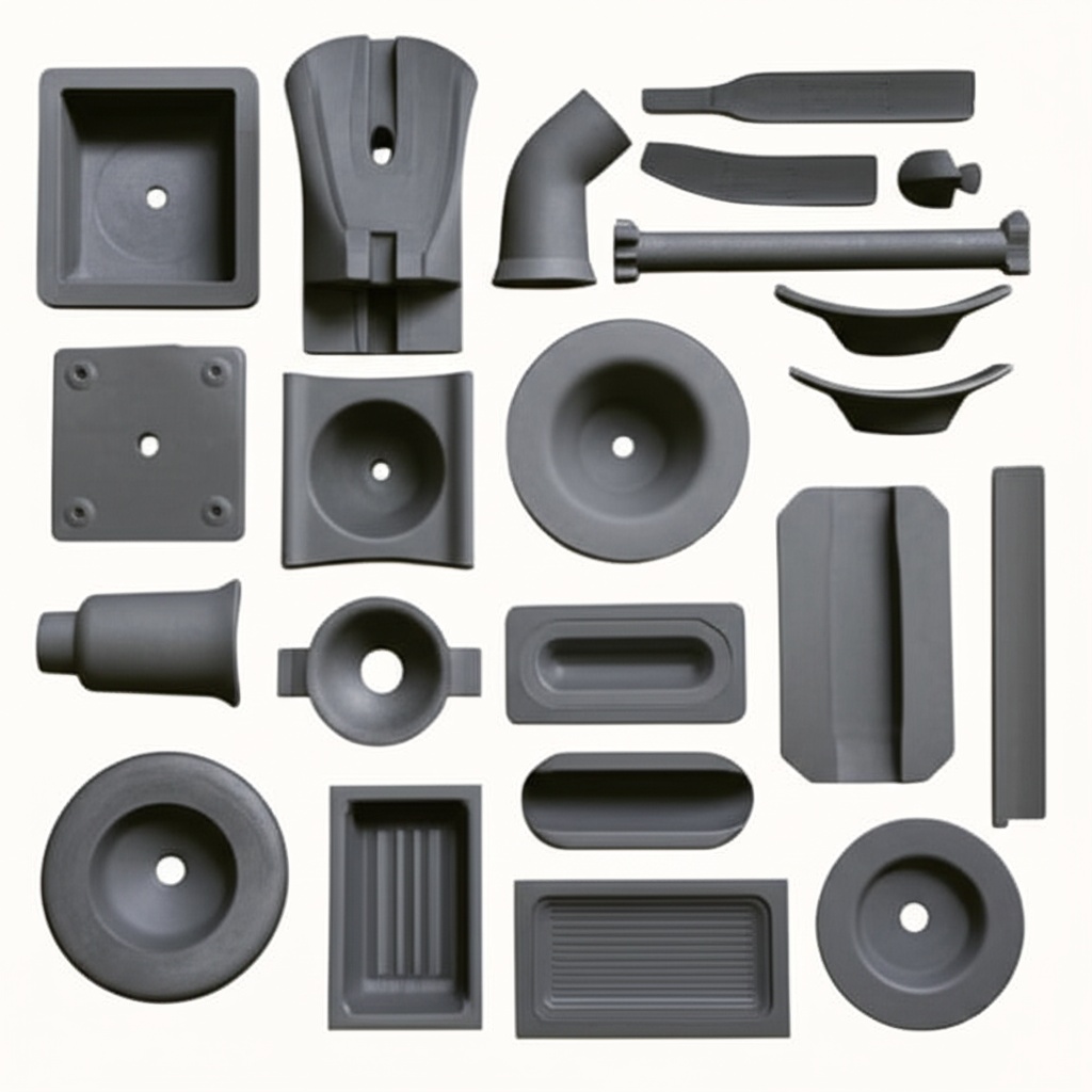
Customizable SiC
You May Also Interest
-
![]()
Stock Up on SiC Spare Parts for Maximum Uptime
Stock Up on SiC Spare Parts for Maximum Uptime In today’s demanding industrial landscape, where precision, reliability, and extreme performance are paramount, the longevity of critical equipment directly impacts productivity and profitability. Downtime due to component failure can be incredibly costly. This is where high-quality silicon carbide (SiC) spare parts become indispensable. Known for their…
-
![]()
Unlocking Peak Performance: The Indispensable Role of Custom Silicon Carbide Discs in Demanding Industries
In the relentless pursuit of efficiency, durability, and performance, advanced materials play a pivotal role. Among these, silicon carbide (SiC) stands out as a material of exceptional capabilities. Specifically, custom silicon carbide discs are becoming increasingly essential components across a multitude of high-performance industrial applications. These are not mere off-the-shelf parts; they are precision-engineered solutions…
-
![]()
Essential SiC Consumables for Daily Operations
Essential SiC Consumables for Daily Operations In today’s demanding industrial landscape, the performance and longevity of critical components are paramount. For industries pushing the boundaries of temperature, wear, and chemical resistance, traditional materials often fall short. This is where silicon carbide (SiC) consumables emerge as indispensable. As a leading technical content writer for a company…