Silicon Carbide Crystal Growth and Epitaxy Equipment for Wafer Production and Power Device Fabrication
Share
Building Pakistan’s SiC Supply Chain: From Boule to Device in 2025
As Pakistan’s textile, cement, and steel sectors digitize operations and renewable capacity surges in Sindh and Balochistan, demand for high-efficiency, high-reliability power electronics is accelerating. Localizing parts of the silicon carbide (SiC) value chain—crystal growth, epitaxy, wafering, and device fabrication—reduces foreign exchange exposure, shortens lead times, and enables tailored devices for weak-grid conditions. Sicarb Tech provides turnkey SiC crystal growth and epitaxy equipment, process know-how, and factory establishment services, enabling partners to produce 150–200 mm wafers and high-yield epitaxial layers for MOSFETs, Schottky diodes, and power modules used in SVG/STATCOM, APF, VFD front ends, and UPS.
Our systems are engineered for 2025 manufacturing benchmarks: high-yield 4H-SiC boules, low micropipe density substrates, epi thickness/uniformity optimized for 1200/1700 V devices, and in-line metrology for consistent electrical performance. Backed by the Chinese Academy of Sciences, Sicarb Tech’s technology transfer closes the capability gap so Pakistani enterprises can advance from materials to qualified devices aligned with IEEE/IEC-driven market requirements.
Technical Specifications and Advanced Features
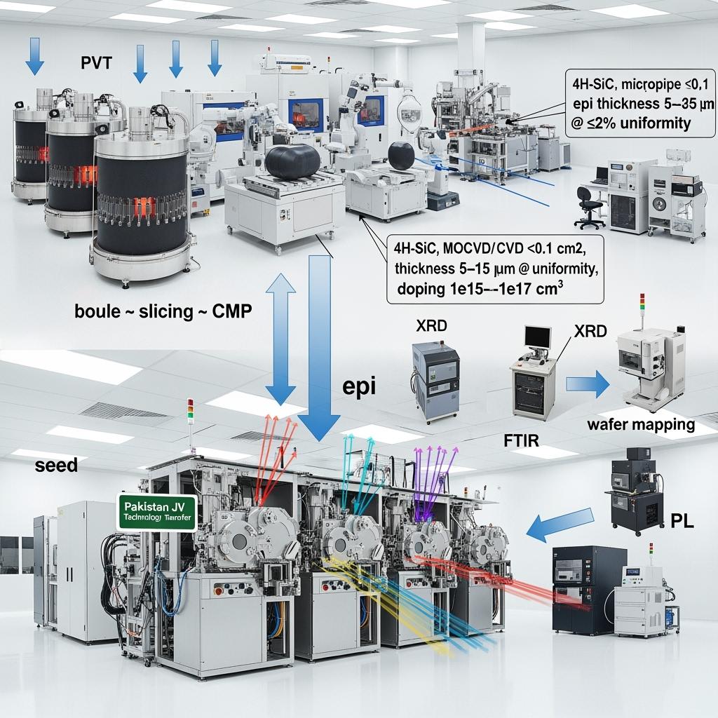
- Crystal growth (PVT/modified Lely)
- 4H-SiC boules, 150 mm standard; 200 mm roadmap with seed alignment control
- Micropipe density: <0.1 cm⁻²; basal plane dislocation (BPD) conversion strategies
- Temperature control: 2200–2400°C with multi-zone profiling; thermal gradient optimization for low defect density
- Graphite/SiC-coated hot-zone components for longevity and purity
- Wafering and surface prep
- Precision ID/dicing saws with low-damage slicing; laser scribing options
- Double-side grinding and CMP achieving Ra <0.1 nm and TTV <5 µm (150 mm)
- Wafer cleanliness: metallic contamination control with advanced wet benches
- Epitaxy (CVD/MOCVD for 4H-SiC)
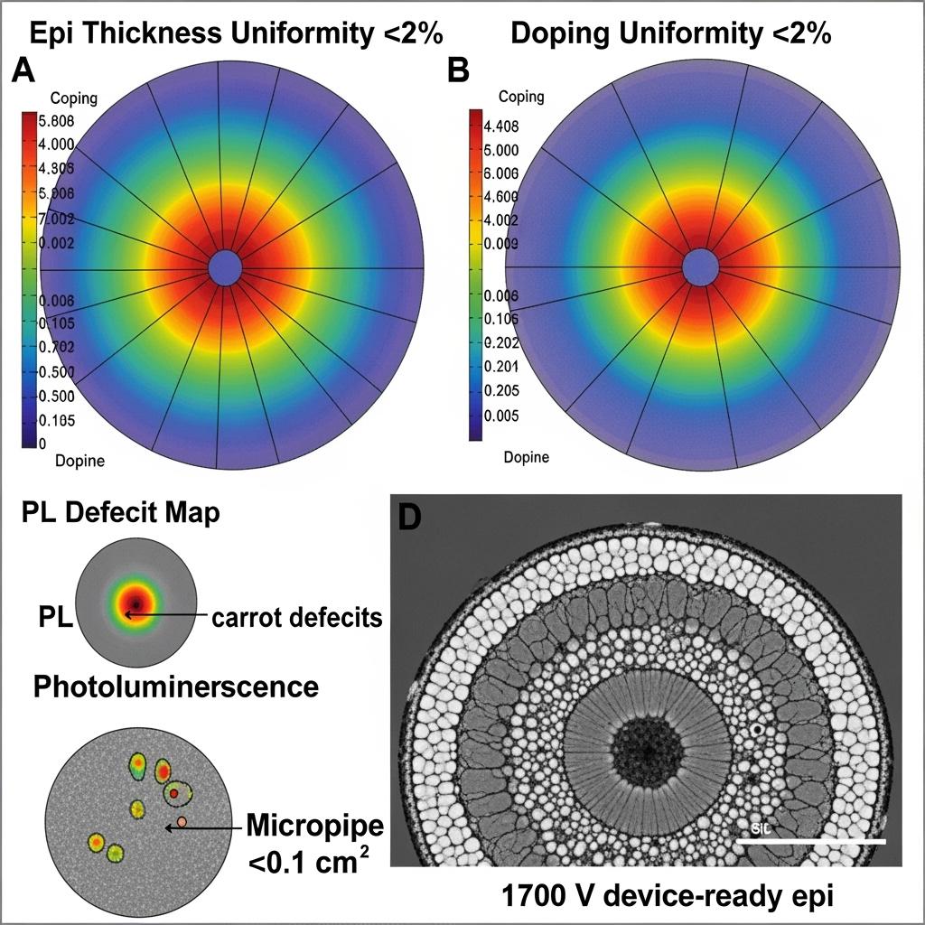
- Thickness: 2–30 µm typical (devices: 5–15 µm for 1200/1700 V), uniformity ≤±2% (within-wafer)
- Doping: n-type 1e15–1e17 cm⁻³; p-type optional for JBS/PN structures
- Defect control: in-situ gas modulation for epi defect reduction (triangles, carrots, stacking faults)
- Reactor features: susceptor temperature uniformity, optimized gas delivery (SiH4, C3H8, H2), in-situ pyrometry/reflectometry
- In-line metrology and quality
- XRD rocking curve, FTIR thickness mapping, AFM for roughness, PL for defect mapping
- Wafer maps integrated to MES with SPC/DOE capabilities
- Traceability for yield learning, aligned with ISO 9001/14001 frameworks
- Facilities and safety
- Gas cabinets with interlocks; H2/HCl/Si precursors containment per SEMI/Safety standards
- Exhaust and abatement systems; cleanroom ISO Class 6–7 typical for epi areas
- Localized utility designs for Pakistan: robust power backup, water conservation, and HVAC optimization
Epi and Crystal Growth Platform Advantages for 2025 Manufacturing Readiness
| Capability for local wafer/device supply | Sicarb Tech SiC crystal growth & epitaxy line | Import-only wafer/device sourcing | Impact for Pakistan industry |
|---|---|---|---|
| Lead time and FX exposure | Localizable production with buffered stock | Long lead, FX volatility | Faster deployments, budget certainty |
| Device customization | Epi thickness/doping tailored to SVG/APF/VFD needs | Limited standard options | Better efficiency, reliability |
| Yield learning | In-line metrology + SPC/DOE | Minimal process visibility | Continuous improvement, higher yield |
| Cost over time | Capex + declining unit cost with scale | Persistent premium pricing | Competitive TCO and ROI |
| Strategic capability | Technology transfer and workforce upskilling | Dependency on imports | National resilience and talent growth |
Key Advantages and Proven Benefits
- Device-optimized epi: Thickness and doping profiles engineered for 1200/1700 V MOSFETs and SBDs reduce on-resistance and leakage, enabling 98%+ converter efficiency.
- Quality and yield: Low micropipe and defect densities improve device yield, reducing scrap and cost per ampere.
- Faster product cycles: Onsite epi tuning shortens iterations for APF/STATCOM requirements in weak-grid conditions.
- Turnkey ramp: Integrated utilities, abatement, MES, and training accelerate time-to-qualification.
Expert quote:
“Epitaxy quality—especially thickness uniformity, defect density, and doping precision—directly determines SiC device performance and yield.” — Synthesized from IEEE Electron Devices Society publications on SiC epitaxy control (https://eds.ieee.org/)
“Local value-chain capability reduces supply risk and speeds innovation cycles in power electronics.” — International Energy Agency technology insights on clean energy supply chains (https://www.iea.org/)
Real-World Applications and Measurable Success Stories
- Composite case (regional partnership): Transitioning to locally grown 4H-SiC wafers with tuned epi for 1700 V devices enabled STATCOM modules to lift switching frequency from 20 to 60 kHz, improving var response to <10 ms and total system efficiency to 98.5%.
- Industrial APF optimization: Custom 8–12 µm epi layers with tight uniformity enabled APF modules to achieve >90% harmonic suppression with reduced filter size, cutting cabinet volume by ~30% for textile facilities.
- Reliability uplift: Lower epi defectivity correlated with a 25% increase in device lifetime under high-temperature reverse bias, critical for cement plant auxiliaries.
Selection and Maintenance Considerations
- Capacity planning
- Choose furnace/epi reactor counts based on wafer starts/month and product mix (1200 vs 1700 V)
- Plan for 150 mm now with 200 mm upgradability in tooling and metrology
- Process integration
- Align wafering/CMP specs to epi requirements (TTV, bow, warp)
- Establish SPC with control charts for thickness, doping, and defect density
- Utilities and safety
- Ensure stable power and backup in industrial parks; design gas abatement and monitoring per international best practice
- Train EHS teams on hazardous gases and high-temperature operations
- Supply chain and spares
- Maintain graphite hot-zone spare sets; secure precursor gas contracts
- Calibrate metrology quarterly; maintain MES and recipe change control
Industry Success Factors and Customer Testimonials
- Early feasibility including PKR/USD sensitivity, utility loads, and staffing
- Joint process development with Sicarb Tech to meet end-device KPIs (RDS(on), Qc, leakage)
- Robust qualification plan: monitor HTRB/HTGB, dynamic RDS(on), and avalanche stress on pilot lots
Customer voice (composite):
“Bringing epi capability in-house shortened our device development cycles by months and stabilized supply for our STATCOM/APF lines.” — Technical Director, Power Electronics Manufacturer, South Asia
Future Innovations and Market Trends (2025+)
- 200 mm 4H-SiC maturation: Scaling reactors and metrology to maintain uniformity and defectivity
- Epi advances: Lower-temperature growth, chlorine chemistries for higher growth rates, and advanced doping control
- Defect reduction: Conversion of BPDs and mitigation of stacking faults for higher-voltage devices
- Integration with device fabs: Inline wafer-level reliability screening and digital twins for process optimization
- Pakistan opportunity: CPEC-driven industrial parks and SEZs enabling clustered SiC ecosystems with shared utilities and talent pipelines
Common Questions and Expert Answers
- What wafer sizes are supported today?
150 mm production-ready with a roadmap to 200 mm; equipment and metrology are upgradable. - What epi specs are typical for 1700 V devices?
Thickness 10–15 µm, n-type doping ~1e15–5e15 cm⁻³ with ≤±2% uniformity and low defectivity. - How long to ramp from installation to qualified wafers?
Typically 6–9 months including installation, process transfer, pilot lots, and reliability qualification (HTRB/HTGB). - What facilities are required?
Cleanroom ISO Class 6–7 for epi, high-purity gases with abatement, reliable power/HVAC, and wet process tools for wafer prep. - Can Sicarb Tech support technology transfer and training?
Yes—complete packages include recipes, SOPs, equipment specs, SPC/DOE methodologies, and hands-on training/qualification.
Why This Solution Works for Your Operations
Local or regional SiC crystal growth and epitaxy create strategic control over critical power electronics components. With Sicarb Tech’s proven equipment and process IP, Pakistani manufacturers can deliver customized, high-yield wafers tailored to weak-grid realities—improving converter efficiency, reliability, and time-to-market while reducing FX and lead-time risks.
Connect with Specialists for Custom Solutions
Accelerate your SiC manufacturing journey with Sicarb Tech:
- 10+ years of SiC manufacturing expertise
- Chinese Academy of Sciences backing and innovation
- Custom product development across R‑SiC, SSiC, RBSiC, SiSiC and power device platforms
- Technology transfer and factory establishment services: feasibility, layout, installation, commissioning
- Turnkey solutions from materials and substrates to epitaxy, device test, and module packaging
- Proven track record with 19+ enterprises delivering measurable performance and ROI
Request a free feasibility study, capacity model, and phased ramp plan tailored to your site.
Email: [email protected] | Phone/WhatsApp: +86 133 6536 0038
Article Metadata
- Last updated: 2025-09-11
- Next scheduled update: 2025-12-15
- Prepared by: Sicarb Tech SiC Manufacturing Solutions Team
- References: IEEE Electron Devices Society resources on SiC epitaxy; SEMI safety guidance; IEEE 519/IEC 61000-3-6 for downstream applications; IEA clean energy supply chain insights; Sicarb Tech internal process documentation (available under NDA)

About the Author: Sicarb Tech
We provide clear and reliable insights into silicon carbide materials, component manufacturing, application technologies, and global market trends. Our content reflects industry expertise, practical experience, and a commitment to helping readers understand the evolving SiC landscape.

Customizable SiC
You May Also Interest
-
![]()
SiC Substrates: Key to Electronic Device Advances
SiC Substrates: Key to Electronic Device Advances Introduction: The Pivotal Role of SiC Substrates In the rapidly evolving landscape of high-performance industrial applications, materials science plays a crucial role. Among advanced materials, silicon carbide (SiC) stands out, particularly in the form of SiC substrates. These substrates are not merely foundational layers; they are critical enablers…
-
![]()
SiC Innovation via University Research Links
SiC Innovation via University Research Links In the rapidly evolving landscape of advanced materials, custom silicon carbide (SiC) stands out as a true game-changer. Its unparalleled properties make it indispensable across a spectrum of demanding industrial applications, from the cutting edge of semiconductor manufacturing to the extreme environments of aerospace and nuclear energy. But what…
-
![]()
Next-Gen SiC Wafers for Power Electronics Excellence
Next-Gen SiC Wafers for Power Electronics Excellence Introduction: The Pivotal Role of SiC Wafers in Modern Power Electronics The relentless pursuit of higher efficiency, increased power density, and superior performance in power electronic systems has spotlighted silicon carbide (SiC) as a transformative material. SiC wafers, the foundational substrates for SiC-based power devices, are at the…